
Datasheet


Microprocessor
Supervisory Circuits
Data Sheet
ADM8690/ADM8691/ADM8695
Rev. C
Information furnished by Analog Devices is believed to be accurate and reliable. However, no
responsibility is assumed by Analog Devices for its use, nor for any infringements of patents or other
rights of third parties that may result from its use. Specifications subject to change without notice. No
license is granted by implication or otherwise under any patent or patent rights of Analog Devices.
Trademarks and registered trademarks are the property of their respective owners.
One Technology Way, P.O. Box 9106, Norwood, MA 02062-9106, U.S.A.
Tel: 781.329.4700 www.analog.com
Fax: 781.461.3113 ©2006–2011 Analog Devices, Inc. All rights reserved.
FEATURES
Upgrade for the ADM690, ADM691, ADM695 and
for the MAX690, MAX691, MAX695
Specified over temperature
Low power consumption: 0.7 mW
Precision voltage monitor
Reset assertion down to 1 V V
CC
Low switch on resistance: 0.7 Ω normal, 7 Ω in backup
High current drive: 100 mA
Watchdog timer: 100 ms, 1.6 sec, or adjustable
Standby current: 400 nA
Automatic battery backup power switching
Extremely fast gating of chip enable signals (3 ns)
Voltage monitor for power fail
Available in TSSOP package
APPLICATIONS
Microprocessor systems
Computers
Controllers
Intelligent instruments
Automotive systems
PRODUCT HIGHLIGHTS
The ADM8690 is available in 8-lead PDIP and SOIC packages
and provides the following functions:
1. Power-on reset output during power-up, power-down,
and brownout conditions. The
RESET
output remains
operational with V
CC
as low as 1 V.
2. Battery backup switching for CMOS RAM, CMOS micro-
processor, or other low power logic.
3. Reset pulse if the optional watchdog timer is not toggled
within a specified time.
4. 1.3 V threshold detector for power-fail warning, low battery
detection, or to monitor a power supply other than 5 V.
The ADM8691 and ADM8695 are available in 16-lead PDIP
and small outline packages (including TSSOP) and provide
three additional functions:
1. Write protection of CMOS RAM or EEPROM.
2. Adjustable reset and watchdog timeout periods.
3. Separate watchdog timeout, backup battery switchover, and
low V
CC
status outputs.
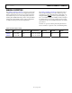
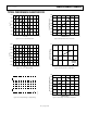
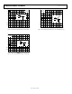
FUNCTIONAL BLOCK DIAGRAMS
RESET
1.3V
RESET
GENERATOR
2
WATCHDOG
TRANSITION DETECTOR
(1.6sec)
4.65V
1
ADM8690
WATCHDOG
INPUT (WDI)
POWER-FAIL
POWER-FAIL
INPUT (PFI)
V
CC
V
BATT
V
OUT
OUTPUT (PFO)
1
VOLTAGE DETECTOR = 4.65V
2
RESET PULSE WIDTH = 50ms
00093-001
Figure 1. ADM8690
1.3V
LOW LINE
RESET
RESET
OSC IN
OSC SEL
B
A
TT ON
ADM8691/
ADM8695
4.65V
1
RESET AND
WATCHDOG
TIME BASE
RESET
GENERATOR
WATCHDOG
TRANSITION DETECTOR
WATCHDOG
TIMER
POWER-FAIL
INPUT (PFI)
WATCHDOG
INPUT (WDI)
V
BATT
V
OUT
POWER-FAIL
OUTPUT (PFO)
WATCHDOG
OUTPUT (WDO)
CE
OUT
1
VOLTAGE DETECTOR = 4.65V
CE
IN
V
CC
00093-002
Figure 2. ADM8691/ADM8695