
Datasheet


ADM8690/ADM8691/ADM8695 Data Sheet
Rev. C | Page 6 of 24
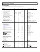
ABSOLUTE MAXIMUM RATINGS
T
A
= 25°C, unless otherwise noted.
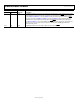
Table 3.
Parameter Rating
V
CC
−0.3 V to +6 V
V
BATT
−0.3 V to +6 V
All Other Inputs −0.3 V to V
OUT
+ 0.5 V
Input Current
V
CC
200 mA
V
BATT
50 mA
GND 20 mA
Digital Output Current 20 mA
Power Dissipation, 8-Lead PDIP 400 mW
θ
JA
Thermal Impedance 120°C/W
Power Dissipation, 8-Lead SOIC 400 mW
θ
JA
Thermal Impedance 120°C/W
Power Dissipation, 16-Lead PDIP 600 mW
θ
JA
Thermal Impedance 135°C/W
Power Dissipation, 16-Lead TSSOP 600 mW
θ
JA
Thermal Impedance 158°C/W
Power Dissipation, 16-Lead SOIC_N 600 mW
θ
JA
Thermal Impedance 110°C/W
Power Dissipation, 16-Lead SOIC_W 600 mW
θ
JA
Thermal Impedance 73°C/W
Operating Temperature Range
Industrial (A Version) −40°C to +85°C
Lead Temperature (Soldering, 10 sec) 300°C
Storage Temperature Range −65°C to +150°C
Stresses above those listed under Absolute Maximum Ratings
may cause permanent damage to the device. This is a stress
rating only; functional operation of the device at these or any
other conditions above those indicated in the operational
section of this specification is not implied. Exposure to absolute
maximum rating conditions for extended periods may affect
device reliability.
ESD CAUTION