
Datasheet


ADN2813
Rev. B | Page 6 of 28
ABSOLUTE MAXIMUM RATINGS
T
A
= T
MIN
to T
MAX
, VCC = V
MIN
to V
MAX
, VEE = 0 V, C
F
=
0.47 μF, SLICEP = SLICEN = VEE, unless otherwise noted.
THERMAL CHARACTERISTICS
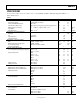
Table 4.
Parameter Rating
Supply Voltage (VCC) 4.2 V
Minimum Input Voltage (All Inputs) VEE − 0.4 V
Maximum Input Voltage (All Inputs) VCC + 0.4 V
Maximum Junction Temperature 125°C
Storage Temperature Range −65°C to +150°C
Thermal Resistance
32-LFCSP, 4-layer board with exposed paddle soldered to VEE,
θ
JA
= 28°C/W.
Stress above those listed under Absolute Maximum Ratings may
cause permanent damage to the device. This is a stress rating
only and functional operation of the device at these or any other
conditions above those indicated in the operational sections of
this specification is not implied. Exposure to absolute
maximum rating conditions for extended periods may affect
device reliability.
ESD CAUTION
ESD (electrostatic discharge) sensitive device. Electrostatic charges as high as 4000 V readily accumulate on
the human body and test equipment and can discharge without detection. Although this product features
proprietary ESD protection circuitry, permanent damage may occur on devices subjected to high energy
electrostatic discharges. Therefore, proper ESD precautions are recommended to avoid performance
degradation or loss of functionality.