
Datasheet


ADN2814 Data Sheet
Rev. C | Page 2 of 28
TABLE OF CONTENTS
Features .............................................................................................. 1
Applications....................................................................................... 1
General Description......................................................................... 1
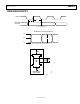
Functional Block Diagram .............................................................. 1
Revision History ............................................................................... 2
Specifications..................................................................................... 3
Jitter Specifications....................................................................... 4
Output and Timing Specifications............................................. 5
Absolute Maximum Ratings............................................................ 6
Thermal Characteristics .............................................................. 6
ESD Caution.................................................................................. 6
Timing Characteristics..................................................................... 7
Pin Configuration and Function Descriptions............................. 8
Typical Performance Characteristics ............................................. 9
I
2
C Interface Timing and Internal Register Description........... 10
Terminology .................................................................................... 12
Jitter Specifications......................................................................... 13
Theory of Operation ...................................................................... 14
Functional Description.................................................................. 16
Frequency Acquisition............................................................... 16
Limiting Amplifier ..................................................................... 16
Slice Adjust.................................................................................. 16
Loss-of-Signal (LOS) Detector ................................................. 16
Lock Detector Operation .......................................................... 17
Harmonic Detector .................................................................... 17
SQUELCH Mode........................................................................ 18
I
2
C Interface ................................................................................ 18
Reference Clock (Optional) ...................................................... 18
Applications Information.............................................................. 21
PCB Design Guidelines ............................................................. 21
DC-Coupled Application .......................................................... 23
Coarse Data Rate Readback Look-Up Table............................... 24
Outline Dimensions ....................................................................... 26
Ordering Guide .......................................................................... 26
REVISION HISTORY
3/12—Rev. B to Rev. C
Updated Outline Dimensions....................................................... 26
Changes to Ordering Guide .......................................................... 26
5/10—Rev. A to Rev. B
Changes to Figure 5 and Table 5..................................................... 8
Changes to Figure 24...................................................................... 21
Added Exposed Pad Notation to Outline Dimensions ............. 26
3/09—Rev. 0 to Rev. A
Updated Outline Dimensions....................................................... 26
Changes to Ordering Guide .......................................................... 26
9/05—Revision 0: Initial Version