
Datasheet


Data Sheet ADN2816
Rev. C | Page 11 of 24
JITTER SPECIFICATIONS
The ADN2816 CDR is designed to achieve the best bit-error-
rate (BER) performance and to exceed the jitter transfer,
generation, and tolerance specifications proposed for
SONET/SDH equipment defined in the Telcordia Technologies
specification.
Jitter is the dynamic displacement of digital signal edges from
their long-term average positions, measured in unit intervals
(UI), where 1 UI = 1 bit period. Jitter on the input data can
cause dynamic phase errors on the recovered clock sampling
edge. Jitter on the recovered clock causes jitter on the
retimed data.
The following sections briefly summarize the specifications of
jitter generation, transfer, and tolerance in accordance with the
Telcordia document (GR-253-CORE, Issue 3, September 2000)
for the optical interface at the equipment level and the
ADN2816 performance with respect to those specifications.
Jitter Generation
The jitter generation specification limits the amount of jitter
that can be generated by the device with no jitter and wander
applied at the input. For SONET devices, the jitter generated
must be less than 0.01 UI rms, and must be less than 0.1 UI p-p.
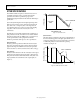
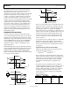
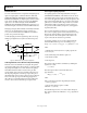
Jitter Transfer
The jitter transfer function is the ratio of the jitter on the output
signal to the jitter applied on the input signal vs. the frequency.
This parameter measures the limited amount of the jitter on an
input signal that can be transferred to the output signal (see
Figure 11).
04948-0-015
0.1
ACCEPTABLE
RANGE
f
C
JITTER FREQUENCY (kHz)
SLOPE = –20dB/DECADE
JITTER GAIN (dB)
Figure 11. Jitter Transfer Curve
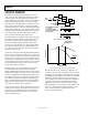
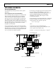
Jitter Tolerance
The jitter tolerance is defined as the peak-to-peak amplitude of
the sinusoidal jitter applied on the input signal, which causes a
1 dB power penalty. This is a stress test intended to ensure that
no additional penalty is incurred under the operating
conditions (see Figure 12).
04948-0-016
15.00
1.50
0.15
f
0
f
1
f
2
f
3
f
4
JITTER FREQUENCY (kHz)
SLOPE = –20dB/DECADE
INPUT JITTER AMPLITUDE (UI p-p)
Figure 12. SONET Jitter Tolerance Mask