
Datasheet
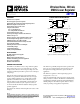
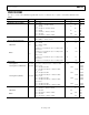
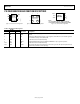
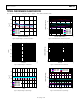
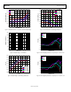
Table Of Contents
- Features
- Applications
- Typical Application Circuit
- General Description
- Revision History
- Specifications
- Absolute Maximum Ratings
- Pin Configurations and Function Descriptions
- Typical Performance Characteristics
- Theory of Operation
- Applications Information
- Printed Circuit Board Layout Considerations
- Outline Dimensions
Ultralow Noise, 200 mA,
CMOS Linear Regulator
Data Sheet
ADP151
Rev. E
Information furnished by Analog Devices is believed to be accurate and reliable. However, no
responsibility is assumed by Analog Devices for its use, nor for any infringements of patents or other
rights of third parties that may result from its use. Specifications subject to change without notice. No
license is granted by implication or otherwise under any patent or patent rights of Analog Devices.
Trademarks and registered trademarks are the property of their respective owners.
One Technology Way, P.O. Box 9106, Norwood, MA 02062-9106, U.S.A.
Tel: 781.329.4700
www.analog.com
Fax: 781.461.3113 ©2010–2012 Analog Devices, Inc. All rights reserved.
FEATURES
Ultralow noise: 9 µV rms
No noise bypass capacitor required
Stable with 1 µF ceramic input and output capacitors
Maximum output current: 200 mA
Input voltage range: 2.2 V to 5.5 V
Low quiescent current
I
GND
= 10 µA with 0 load
I
GND
= 265 μA with 200 mA load
Low shutdown current: <1 µA
Low dropout voltage: 140 mV at 200 mA load
Initial accuracy: ±1%
Accuracy over line, load, and temperature: ±2.5%
16 fixed output voltage options: 1.1 V to 3.3 V
PSRR performance of 70 dB at 10 kHz
Current-limit and thermal overload protection
Logic controlled enable
Internal pull-down resistor on EN input
5-lead TSOT package
6-lead LFCSP package
4-ball, 0.4 mm pitch WLCSP
APPLICATIONS
RF, VCO, and PLL power supplies
Mobile phones
Digital camera and audio devices
Portable and battery-powered equipment
Post dc-to-dc regulation
Portable medical devices
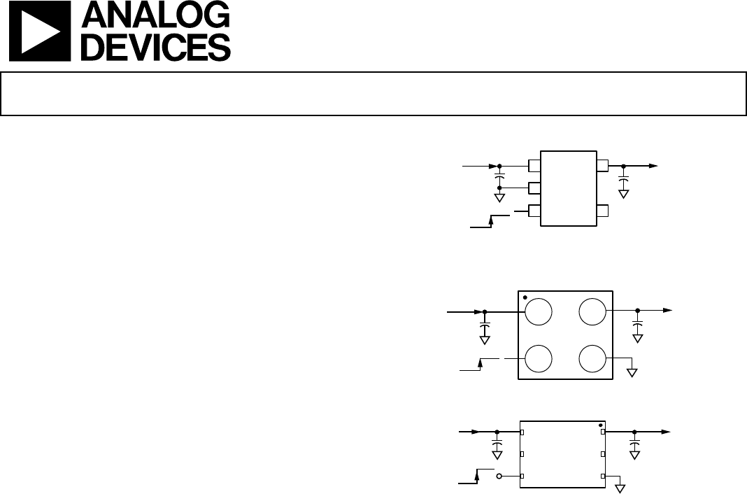
TYPICAL APPLICATION CIRCUIT
NC = NO CONNECT
1
2
3
5
4
1µF
1µF
V
OUT
= 1.8VV
IN
= 2.3V
VOUT
NC
VIN
GND
EN
OFF
ON
08627-001
Figure 1. TSOT ADP151 with Fixed Output Voltage, 1.8 V
VIN VOUT
1 2
EN GND
C
OUT
1µF
C
IN
V
OUT
= 1.8V
V
IN
= 2.3V
TOP VIEW
(Not to Scale)
A
B
OFF
ON
08627-002
Figure 2. WLCSP ADP151 with Fixed Output Voltage, 1.8 V
ADP151
TOP VIEW
(Not to Scale)
4
6
5
GND
VOUT
NC
3
1
2
EN
VIN
NC
08627-047
NC = NO CONNECT. DO NOT
CONNECT TO THIS PIN.
ON
OFF
1µF 1µF
V
IN
= 2.3V V
OUT
= 1.8V
Figure 3. LFCSP ADP151 with Fixed Output Voltage, 1.8 V
GENERAL DESCRIPTION
The ADP151 is an ultralow noise, low dropout linear regulator
that operates from 2.2 V to 5.5 V and provides up to 200 mA
of output current. The low 140 mV dropout voltage at 200 mA
load improves efficiency and allows operation over a wide input
voltage range.
Using an innovative circuit topology, the ADP151 achieves
ultralow noise performance without the necessity of a bypass
capacitor, making it ideal for noise-sensitive analog and RF
applications. The ADP151 also achieves ultralow noise per-
formance without compromising PSRR or transient line and
load performance. The low 265 μA of quiescent current at
200 mA load makes the ADP151 suitable for battery-operated
portable equipment.
The ADP151 also includes an internal pull-down resistor on the
EN input.
The ADP151 is specifically designed for stable operation with
tiny 1 µF, ±30% ceramic input and output capacitors to meet
the requirements of high performance, space constrained
applications.
The ADP151 is capable of 16 fixed output voltage options,
ranging from 1.1 V to 3.3 V.
Short-circuit and thermal overload protection circuits prevent
damage in adverse conditions. The ADP151 is available in tiny
5-lead TSOT, 6-lead LFCSP, and 4-ball, 0.4 mm pitch, halide-free
WLCSP packages for the smallest footprint solution to meet a
variety of portable power application requirements.