
Datasheet
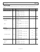
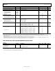
Table Of Contents
- Features
- Applications
- Typical Application Circuit
- General Description
- Revision History
- Specifications
- Absolute Maximum Ratings
- Pin Configurations and Function Descriptions
- Typical Performance Characteristics
- Theory of Operation
- Applications Information
- Printed Circuit Board Layout Considerations
- Outline Dimensions

ADP151 Data Sheet
Rev. E | Page 4 of 24
Parameter Symbol Conditions Min Typ Max Unit
START-UP TIME
3
t
START-UP
V
OUT
= 3.3 V 180 µs
CURRENT-LIMIT THRESHOLD
4
I
LIMIT
T
J
= 0°C to +125°C
220
300
400
mA
UNDERVOLTAGE LOCKOUT T
J
= −40°C to +125°C
Input Voltage Rising UVLO
RISE
1.96 V
Input Voltage Falling UVLO
FAL L
1.28 V
Hysteresis UVLO
HYS
120 mV
THERMAL SHUTDOWN
Thermal Shutdown Threshold
TS
SD
T
J
rising
150
°
C
Thermal Shutdown Hysteresis TS
SD-HYS
15
°C
EN INPUT
EN Input Logic High V
IH
2.2 V ≤ V
IN
≤ 5.5 V 1.2 V
EN Input Logic Low V
IL
2.2 V ≤ V
IN
≤ 5.5 V 0.4 V
EN Input Pull-Down Resistance R
EN
V
IN
= V
EN
= 5.5 V 2.6 MΩ
OUTPUT NOISE OUT
NOISE
10 Hz to 100 kHz, V
IN
= 5 V, V
OUT
= 3.3 V 9 µV rms
10 Hz to 100 kHz, V
IN
= 5 V, V
OUT
= 2.5 V 9 µV rms
10 Hz to 100 kHz, V
IN
= 5 V, V
OUT
= 1.1 V 9 µV rms
POWER SUPPLY REJECTION RATIO PSRR
V
IN
= V
OUT
+ 0.5 V 10 kHz, V
IN
= 3.8 V, V
OUT
= 3.3 V, I
OUT
= 10 mA 70 dB
100 kHz, V
IN
= 3.8 V, V
OUT
= 3.3 V, I
OUT
= 10 mA 55 dB
V
IN
= V
OUT
+ 1 V 10 kHz, V
IN
= 4.3 V, V
OUT
= 3.3 V, I
OUT
= 10 mA 70 dB
100 kHz, V
IN
= 4.3 V, V
OUT
= 3.3 V, I
OUT
= 10 mA
55
dB
10 kHz, V
IN
= 2.2 V, V
OUT
= 1.1 V, I
OUT
= 10 mA 70 dB
100 kHz, V
IN
= 2.2 V, V
OUT
= 1.1 V, I
OUT
= 10 mA 55 dB
1
Based on an end-point calculation using 0.1 mA and 200 mA loads. See Figure 8 for typical load regulation performance for loads less than 1 mA.
2
Dropout voltage is defined as the input-to-output voltage differential when the input voltage is set to the nominal output voltage. This applies only for output
voltages above 2.2 V.
3
Start-up time is defined as the time between the rising edge of EN and V
OUT
being at 90% of its nominal value.
4
Current-limit threshold is defined as the current at which the output voltage drops to 90% of the specified typical value. For example, the current limit for a 3.0 V
output voltage is defined as the current that causes the output voltage to drop to 90% of 3.0 V (that is, 2.7 V).
INPUT AND OUTPUT CAPACITOR, RECOMMENDED SPECIFICATIONS
Table 2.
Parameter Symbol Conditions Min Typ Max Unit
Minimum Input and Output
Capacitance
1
C
MIN
T
A
= −40°C to +125°C 0.7 µF
Capacitor ESR R
ESR
T
A
= −40°C to +125°C 0.001 0.2 Ω
1
The minimum input and output capacitance should be greater than 0.7 μF over the full range of operating conditions. The full range of operating conditions in the
application must be considered during device selection to ensure that the minimum capacitance specification is met. X7R and X5R type capacitors are recommended;
Y5V and Z5U capacitors are not recommended for use with any LDO.