
Datasheet
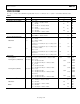
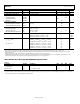
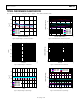
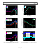
Table Of Contents
- Features
- Applications
- Typical Application Circuit
- General Description
- Revision History
- Specifications
- Absolute Maximum Ratings
- Pin Configurations and Function Descriptions
- Typical Performance Characteristics
- Theory of Operation
- Applications Information
- Printed Circuit Board Layout Considerations
- Outline Dimensions

ADP151 Data Sheet
Rev. E | Page 6 of 24
PIN CONFIGURATIONS AND FUNCTION DESCRIPTIONS
NC = NO CONNECT
TOP VIEW
(Not to Scale)
ADP151
1
2
3
5
4
VIN
GND
EN
VOUT
NC
08627-003
1 2
A
B
TOP VIEW
(Not to Scale)
VIN VOUT
EN GND
08627-004
ADP151
TOP VIEW
(Not to Scale)
3
1
2
GND
VOUT
NC
4
6
5
EN
VIN
NC
08627-048
NOTES
1. NC = NO CONNECT. DO NOT CONNECT TO THIS PIN.
2. THE EXPOSED PAD MUST BE CONNECTED TO GROUND.
Figure 4. 5-Lead TSOT Pin Configuration Figure 5. 4-Ball WLCSP Pin Configuration Figure 6. 6-Lead LFCSP Pin Configuration
Table 5. Pin Function Descriptions
Pin No.
Mnemonic Description
TSOT WLCSP LFCSP
1 A1 6 VIN Regulator Input Supply. Bypass VIN to GND with a 1 µF or greater capacitor.
2 B2 3 GND Ground.
3
B1
4
EN
Enable Input. Drive EN high to turn on the regulator; drive EN low to turn off the regulator.
For automatic startup, connect EN to VIN.
4 N/A 2 NC No Connect. Not connected internally.
5 A2 1 VOUT Regulated Output Voltage. Bypass VOUT to GND with a 1 µF or greater capacitor.
N/A N/A 5 NC No Connect. Not connected internally.
N/A N/A EPAD Exposed Pad. The exposed pad must be connected to ground. The exposed pad enhances
the thermal performance of the package.