
Datasheet

Data Sheet ADP160/ADP161/ADP162/ADP163
Rev. H | Page 5 of 24
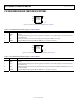
ABSOLUTE MAXIMUM RATINGS
Table 3.
Parameter Rating
VIN to GND −0.3 V to +6.5 V
VOUT to GND −0.3 V to VIN
EN to GND −0.3 V to VIN
ADJ to GND −0.3 V to VIN
NC to GND −0.3 V to VIN
Storage Temperature Range −65°C to +150°C
Operating Junction Temperature Range −40°C to +125°C
Operating Ambient Temperature Range
−40°C to +125°C
Soldering Conditions JEDEC J-STD-020
Stresses above those listed under Absolute Maximum Ratings
may cause permanent damage to the device. This is a stress
rating only; functional operation of the device at these or any
other conditions above those indicated in the operational
section of this specification is not implied. Exposure to absolute
maximum rating conditions for extended periods may affect
device reliability.
THERMAL DATA
Absolute maximum ratings only apply individually; they do not
apply in combination. The ADP16x can be damaged when the
junction temperature limits are exceeded. Monitoring ambient
temperature does not guarantee that T
J
is within the specified
temperature limits. In applications with high power dissipation
and poor thermal resistance, the maximum ambient temperature
may have to be derated.
In applications with moderate power dissipation and low PCB
thermal resistance, the maximum ambient temperature can
exceed the maximum limit as long as the junction temperature
is within specification limits. The junction temperature (T
J
) of
the device is dependent on the ambient temperature (T
A
), the
power dissipation of the device (P
D
), and the junction-to-ambient
thermal resistance of the package (θ
JA
).
Maximum junction temperature (T
J
) is calculated from the ambient
temperature (T
A
) and power dissipation (P
D
) using the formula
T
J
= T
A
+ (P
D
× θ
JA
)
Junction-to-ambient thermal resistance (θ
JA
) of the package is
based on modeling and calculation using a 4-layer board. The
junction-to-ambient thermal resistance is highly dependent on the
application and board layout. In applications where high maximum
power dissipation exists, close attention to thermal board design
is required. The value of θ
JA
may vary, depending on PCB material,
layout, and environmental conditions. The specified values of
θ
JA
are based on a 4-layer, 4 inches × 3 inches, circuit board. Refer
to JESD 51-7 and JESD 51-9 for detailed information on the
board construction. For additional information, see the AN-617
Application Note, MicroCSP™ Wafer Level Chip Scale Package.
Ψ
JB
is the junction to board thermal characterization parameter
with units of °C/W. Ψ
JB
of the package is based on modeling and
calculation using a 4-layer board. The JESD51-12, Guidelines for
Reporting and Using Electronic Package Thermal Information,
states that thermal characterization parameters are not the same
as thermal resistances. Ψ
JB
measures the component power flowing
through multiple thermal paths rather than a single path as in
thermal resistance, θ
JB
. Therefore, Ψ
JB
thermal paths include
convection from the top of the package as well as radiation from
the package, factors that make Ψ
JB
more useful in real-world
applications. Maximum junction temperature (T
J
) is calculated
from the board temperature (T
B
) and power dissipation (P
D
)
using the formula
T
J
= T
B
+ (P
D
× Ψ
JB
)
Refer to JESD51-8 and JESD51-12 for more detailed information
about Ψ
JB
.
THERMAL RESISTANCE
θ
JA
and Ψ
JB
are specified for the worst-case conditions, that is, a
device soldered in a circuit board for surface-mount packages.
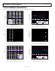
Table 4. Thermal Resistance
Package Type θ
JA
Ψ
JB
Unit
5-Lead TSOT 170 43 °C/W
4-Ball, 0.4 mm Pitch WLCSP 260 58 °C/W
ESD CAUTION