
Datasheet
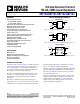

ADP160/ADP161/ADP162/ADP163 Data Sheet
Rev. H | Page 6 of 24
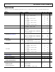
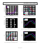
PIN CONFIGURATIONS AND FUNCTION DESCRIPTIONS
NC = NO CONNECT
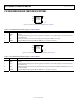
ADP160/
ADP162
TOP VIEW
(Not to Scale)
1
2
3
5
4
VOUT
NC
VIN
GND
EN
08628-004
Figure 4. 5-Lead TSOT, Fixed Output Pin Configuration, ADP160/ADP162
Table 5. 5-Lead TSOT Pin Function Descriptions, ADP160/ADP162
Pin No. Mnemonic Description
1 VIN Regulator Input Supply. Bypass VIN to GND with a 1 μF or greater capacitor.
2 GND Ground.
3 EN
Enable Input. Drive EN high to turn on the regulator; drive EN low to turn off the regulator. For automatic startup,
connect EN to VIN.
4 NC No Connect. This pin is not connected internally. Connect this pin to GND or leave open.
5 VOUT Regulated Output Voltage. Bypass VOUT to GND with a 1 μF or greater capacitor.
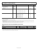
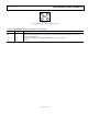
ADP161/
ADP163
TOP VIEW
(Not to Scale)
1
2
3
5
4
VOUT
ADJ
VIN
GND
EN
08628-005
Figure 5. 5-Lead TSOT, Adjustable Output Pin Configuration, ADP161/ADP163
Table 6. 5-Lead TSOT Pin Function Descriptions, ADP161/ADP163
Pin No. Mnemonic Description
1 VIN Regulator Input Supply. Bypass VIN to GND with a 1 μF or greater capacitor.
2 GND Ground.
3 EN
Enable Input. Drive EN high to turn on the regulator; drive EN low to turn off the regulator. For automatic startup,
connect EN to VIN.
4 ADJ
Output Voltage Adjust Pin. Connect the midpoint of the voltage divider between VOUT and GND to this pin to set
the output voltage.
5 VOUT Regulated Output Voltage. Bypass VOUT to GND with a 1 μF or greater capacitor.