
Datasheet


300 mA, Low Quiescent Current,
CMOS Linear Regulators
Data Sheet
ADP170/ADP171
Rev. C Document Feedback
Information furnished by Analog Devices is believed to be accurate and reliable. However, no
responsibility is assumed by Analog Devices for its use, nor for any infringements of patents or other
rights of third parties that may result from its use. Specifications subject to change without notice. No
license is granted by implication or otherwise under any patent or patent rights of Analog Devices.
Trademarks and registered trademarks are the property of their respective owners.
One Technology Way, P.O. Box 9106, Norwood, MA 02062-9106, U.S.A.
Tel: 781.329.4700 ©2009–2014 Analog Devices, Inc. All rights reserved.
Technical Support www.analog.com
FEATURES
Maximum output current: 300 mA
Input voltage range: 1.6 V to 3.6 V
Low quiescent current
I
GND
= 23 µA with 0 mA load
I
GND
= 170 µA with 300 mA load
Low shutdown current: <1 µA
Low dropout voltage: 66 mV at 300 mA load
Output voltage accuracy: ±1%
Up to 31 fixed-output voltage options available from 0.8 V to
3.0 V
Adjustable-output voltage range
0.8 V to 3.0 V (ADP171)
Accuracy over line, load, and temperature: ±3%
Stable with small 1 µF ceramic output capacitor
PSRR performance of 70 dB at 10 kHz and 73 dB at 1 kHz
Low noise: 30 µV rms at V
OUT
= 0.8 V
Current limit and thermal overload protection
Logic-controlled enable
Compact 5-lead TSOT package
APPLICATIONS
Mobile phones
Digital camera and audio devices
Portable and battery-powered equipment
DSP/FPGA/microprocessor supplies
Post dc-dc regulation
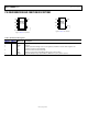
TYPICAL APPLICATION CIRCUITS
07716-001
ADP170
1
2
3
5
4
V
IN
V
OUT
C1 C2
VIN
GND
EN
VOUT
NC
OFF
ON
Figure 1. ADP170 with Fixed Output Voltage, 1.8 V
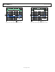
07716-002
ADP171
1
2
3
5
4
V
IN
= 2.3V
V
OUT
= 1.8V
C
IN
1µF
C
OUT
1µF
VIN
GND
EN
VOUT
R1
R2
ADJ
OFF
ON
Figure 2. ADP171 with Adjustable Output Voltage
GENERAL DESCRIPTION
The ADP170/ADP171 are low voltage input, low quiescent
current, low-dropout (LDO) linear regulators that operate from
1.6 V to 3.6 V and provide up to 300 mA of output current. The
low 66 mV dropout voltage at 300 mA load improves efficiency
and allows operation over a wide input voltage range. The low
23 µA of quiescent current at a 0 mA load makes the ADP170/
ADP171 ideal for battery-operated portable equipment.
The ADP170 is capable of 31 fixed-output voltage options, ranging
from 0.8 V t o 3 . 0 V. ADP171 is an adjustable version, which allows
output voltages that range from 0.8 V to 3.0 V via an external
divider. The ADP170/ADP171 are optimized for stable operation
with small 1 µF ceramic output capacitors. Ideal for powering
digital processors, the ADP170/ADP171 exhibit good transient
performance and occupy minimal board space. Compared with
commodity types of LDOs, the ADP170/ADP171 provide 20 dB
to 40 dB better power supply rejection ratio (PSRR) at 100 kHz,
making the ADP170/ADP171 an ideal power source for analog-
to-digital converter (ADC) mixed-signal processor systems and
allowing use of smaller size bypass capacitors. In addition, low
output noise performance without the need for an additional
bypass capacitor further reduces printed circuit board (PCB)
component count.
Short-circuit protection and thermal overload protection circuits
prevent damage in adverse conditions. The ADP170/ADP171
are available in tiny 5-lead TSOT for the smallest footprint
solution to meet a variety of portable power applications.