
Datasheet


ADP170/ADP171 Data Sheet
Rev. C | Page 6 of 20
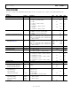
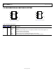
PIN CONFIGURATIONS AND FUNCTION DESCRIPTIONS
ADP170
TOP VIEW
(Not to Scale)
1
2
3
5
4
07716-003
VIN
GND
EN
NC = NO CONNECT
VOUT
NC
Figure 3. ADP170 5-Lead TSOT
ADP171
TOP VIEW
(Not to Scale)
1
2
3
5
4
07716-004
VIN
GND
EN
VOUT
ADJ
Figure 4. ADP171 5-Lead TSOT
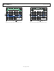
Table 5. Pin Function Descriptions
Pin No.
Mnemonic Description ADP170 ADP171
1 1 VIN Regulator Input Supply. Bypass VIN to GND with a 1 μF or greater capacitor.
2 2 GND Ground.
3 3 EN
Enable Input. Drive EN high to turn on the regulator; drive EN low to turn off the regulator. For
automatic startup, connect EN to VIN.
4 NC No Connect. Not connected internally.
4 ADJ Adjust. A resistor divider from VOUT to ADJ sets the output voltage.
5 5 VOUT Regulated Output Voltage. Bypass VOUT to GND with a 1 μF or greater capacitor.