
Datasheet


ADP1715/ADP1716
Rev. 0 | Page 4 of 20
ABSOLUTE MAXIMUM RATINGS
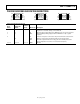
Table 2.
Parameter Rating
IN to GND –0.3 V to +6 V
OUT to GND –0.3 V to IN
EN to GND –0.3 V to +6 V
SS/ADJ/TRK to GND –0.3 V to +6 V
Storage Temperature Range –65°C to +150°C
Operating Junction Temperature Range –40°C to +125°C
Soldering Conditions JEDEC J-STD-020
Stresses above those listed under Absolute Maximum Ratings
may cause permanent damage to the device. This is a stress
rating only; functional operation of the device at these or any
other conditions above those indicated in the operational
section of this specification is not implied. Exposure to absolute
maximum rating conditions for extended periods may affect
device reliability.
THERMAL RESISTANCE
θ
JA
is specified for the worst-case conditions, that is, a device
soldered in a circuit board for surface-mount packages.
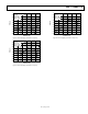
Table 3. Thermal Resistance
Package Type θ
JA
Unit
8-Lead MSOP 118 °C/W
ESD CAUTION