
Datasheet


ADP1715/ADP1716
Rev. 0 | Page 5 of 20
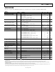
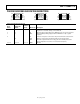
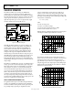
PIN CONFIGURATIONS AND FUNCTION DESCRIPTIONS
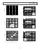
GND
GND
GND
GND
EN
IN
OUT
SS
1
2
3
4
8
7
6
5
ADP1715
FIXED
TOP VIEW
(Not to Scale)
0
6110-004
GND
GND
GND
GND
EN
IN
OUT
ADJ
1
2
3
4
8
7
6
5
ADP1715
ADJUSTABLE
TOP VIEW
(Not to Scale)
0
6110-005
GND
GND
GND
GND
EN
IN
OUT
TRK
1
2
3
4
8
7
6
5
ADP1716
TOP VIEW
(Not to Scale)
0
6110-006
Figure 4. 8-Lead MSOP (RM-Suffix) Figure 5. 8-Lead MSOP (RM-Suffix) Figure 6. 8-Lead MSOP (RM-Suffix)
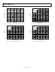
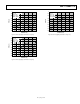
Table 4. Pin Function Descriptions
ADP1715
Fixed
Pin No.
ADP1715
Adjustable
Pin No.
ADP1716
Pin No. Mnemonic Description
1 1 1 EN
Enable Input. Drive EN high to turn on the regulator; drive it low to turn off the
regulator. For automatic startup, connect EN to IN.
2 2 2 IN Regulator Input Supply. Bypass IN to GND with a 2.2 μF or greater capacitor.
3 3 3 OUT
Regulated Output Voltage. Bypass OUT to GND with a 2.2 μF or greater
capacitor.
4 SS Soft Start. A capacitor connected to this pin determines the soft-start time.
4 ADJ Adjust. A resistor divider from OUT to ADJ sets the output voltage.
4 TRK
Track. The output will follow the voltage placed on the TRK pin. (See the
Theory of Operation section for a more detailed description.)
5, 6, 7, 8 5, 6, 7, 8 5, 6, 7, 8 GND Ground.