
Datasheet


ADP1720
Rev. A | Page 10 of 16
THEORY OF OPERATION
The ADP1720 is a low dropout, BiCDMOS linear regulator that
operates from a 4 V to 28 V input rail and provides up to 50 mA
of output current. Ground current in shutdown mode is typically
700 nA. The ADP1720 is stable and provides high power supply
rejection ratio (PSRR) and excellent line and load transient
response with just a small 1 μF ceramic output capacitor.
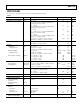
REFERENCE
CURRENT LIMIT
THERMAL PROTECT
SHUTDOWN
OUT
GND/ADJ
IN
EN
19
GND
06111-0
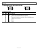
Figure 19. Internal Block Diagram
Internally, the ADP1720 consists of a reference, an error ampli-
fier, a feedback voltage divider, and a DMOS pass transistor.
Output current is delivered via the DMOS pass device, which is
controlled by the error amplifier. The error amplifier compares
the reference voltage with the feedback voltage from the output
and amplifies the difference. If the feedback voltage is lower than
the reference voltage, the gate of the DMOS device is pulled
lower, allowing more current to pass and increasing the output
voltage. If the feedback voltage is higher than the reference
voltage, the gate of the PNP device is pulled higher, allowing
less current to pass and decreasing the output voltage.
The ADP1720 is available in two versions, one with fixed output
voltage options (see Figure 1) and one with an adjustable output
voltage (see Figure 2). The fixed output voltage options are set
internally to either 5.0 V or 3.3 V, using an internal feedback
network. The adjustable output voltage can be set to between
1.225 V and 5.0 V by an external voltage divider connected from
OUT to ADJ. The ADP1720 uses the EN pin to enable and
disable the OUT pin under normal operating conditions. When
EN is high, OUT turns on; when EN is low, OUT turns off. For
automatic startup, EN can be tied to IN.
ADJUSTABLE OUTPUT VOLTAGE
(ADP1720 ADJUSTABLE)
The ADP1720 adjustable version can have its output voltage
set over a 1.225 V to 5.0 V range. The output voltage is set by
connecting a resistive voltage divider from OUT to ADJ. The
output voltage is calculated using the equation
V
OUT
= 1.225 V (1 + R1/R2) (1)
where:
R1 is the resistor from OUT to ADJ.
R2 is the resistor from ADJ to GND.
To make calculation of R1 and R2 easier, Equation 1 can be
rearranged as follows:
R1 = R2 [(V
OUT
/1.225) – 1] (2)
The maximum bias current into ADJ is 100 nA; therefore,
when less than 0.5% error is due to the bias current, use values
less than 60 kΩ for R2.