
Datasheet


ADP1720
Rev. A | Page 12 of 16
THERMAL CONSIDERATIONS
To guarantee reliable operation, the junction temperature of the
ADP1720 must not exceed 125°C. To ensure the junction tem-
perature stays below this maximum value, the user needs to be
aware of the parameters that contribute to junction temperature
changes. These parameters include ambient temperature, power
dissipation in the power device, and thermal resistances between
the junction and ambient air (θ
JA
). The θ
JA
number is dependent
on the package assembly compounds used and the amount of
copper to which the GND pins of the package are soldered on the
PCB. Table 5 shows typical θ
JA
values of the 8-lead MSOP package
for various PCB copper sizes.
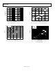
Table 5.
Copper Size (mm
2
)
θ
JA
(°C/W)
0
1
118
50 99
100 77
300 75
500 74
140
0
028
V
IN
– V
OUT
(V)
T
J
(°C)
1
Device soldered to minimum size pin traces.
The junction temperature of the ADP1720 can be calculated
from the following equation:
T
J
= T
A
+ (P
D
× θ
JA
) (3)
where:
T
A
is the ambient temperature.
P
D
is the power dissipation in the die, given by
P
D
= [(V
IN
– V
OUT
) × I
LOAD
] + (V
IN
× I
GND
) (4)
where:
I
LOAD
is the load current.
I
GND
is the ground current.
V
IN
and V
OUT
are input and output voltages, respectively.
Power dissipation due to ground current is quite small and
can be ignored. Therefore, the junction temperature equation
simplifies to the following:
T
J
= T
A
+ {[(V
IN
– V
OUT
) × I
LOAD
] × θ
JA
} (5)
As shown in Equation 5, for a given ambient temperature,
input-to-output voltage differential, and continuous load
current, there exists a minimum copper size requirement for
the PCB to ensure that the junction temperature does not rise
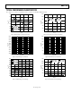
above 125°C. Figure 22 to Figure 27 show junction temperature
calculations for different ambient temperatures, load currents,
V
IN
to V
OUT
differentials, and areas of PCB copper.
120
100
80
60
40
20
1mA
5mA
10mA
20mA
30mA
40mA
50mA
(LOAD CURRENT)
MAX T
J
(DO NOT OPERATE ABOVE THIS POINT)
06111-022
4 8 12 16 20 24
Figure 22. 300 mm
2
of PCB Copper, T
A
= 25°C
140
0
02
V
IN
– V
OUT
(V)
T
J
(°C)
8
120
100
80
60
40
20
1mA
5mA
10mA
20mA
30mA
40mA
50mA
(LOAD CURRENT)
4 8 12 16 20 24
MAX T
J
(DO NOT OPERATE ABOVE THIS POINT)
06111-023
Figure 23. 100 mm
2
of PCB Copper, T
A
= 25°C
140
0
02
V
IN
– V
OUT
(V)
8
(°C)T
J
120
100
80
40
20
60
1mA
5mA
10mA
20mA
30mA
40mA
50mA
(LOAD CURRENT)
4 8 12 16 20 24
MAX T
J
(DO NOT OPERATE ABOVE THIS POINT)
1-0240611
Figure 24. 0 mm
2
of PCB Copper, T
A
= 25°C