
Datasheet


ADP1720
Rev. A | Page 6 of 16
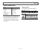
PIN CONFIGURATIONS AND FUNCTION DESCRIPTIONS
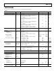
06111-003
GND
GND
GND
ADJ
IN
OUT
GND
GND
GND
GND
IN
OUT
GNDEN
1
2
3
4
8
7
6
5
ADP1720
FIXED
GNDEN
1
2
3
8
7
6
TOP VIEW
(Not to Scale)
4
ADP1720
ADJUSTABLE
TOP VIEW
(Not to Scale)
5
06111-004
Figure 3. 8-Lead MSOP Figure 4. 8-Lead MSOP
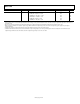
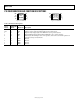
Table 4. Pin Function Descriptions
ADP1720
Fixed
Pin No.
ADP1720
Adjustable
Pin No. Mnemonic Description
1 N/A GND This pin is internally connected to ground.
N/A 1 ADJ Adjust. A resistor divider from OUT to ADJ sets the output voltage.
2 2 IN Regulator Input Supply. Bypass IN to GND with a 1 μF or greater capacitor.
3 3 OUT Regulated Output Voltage. Bypass OUT to GND with a 1 μF or greater capacitor.
4 4 EN
Enable Input. Drive EN high to turn on the regulator; drive it low to turn off the regulator. For
automatic startup, connect EN to IN.
5 5 GND Ground.
6 6 GND Ground.
7 7 GND Ground.
8 8 GND Ground.