
Datasheet
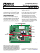


EVAL-ADP1828HC
Rev. 0 | Page 3 of 12
COMPONENT DESIGN
For information in selecting power components and calculating
component values, see the ADP1828 data sheet.
INDUCTOR SELECTION
For this design, a 0.82 µH inductor with a 27 A saturation current
rating (744355182 from Würth Elektronik Group) is selected.
This is a compact flat-wire inductor with a ferrite core, which
offers high performance in terms of low R
DC
and low core loss.
INPUT CAPACITOR
For input voltages up to 18 V and a load up to 20 A, 35 V
multilayer ceramic capacitors (MLCCs) can be used. However,
the 35 V MLCCs are expensive and many of them are needed.
An alternative solution is to use the inexpensive aluminum
electrolytic capacitors, but they are fairly large and bulky and
have large ESR at low temperatures. Another alternative is to
use the OS-CON™ polymer capacitors from Sanyo or the
equivalent from another manufacturer because such capacitors
offer a relative small size, low ESR, and high current ripple rating.
For this design, if the input voltage is 18 V and the inductor is
0.82 µH, the inductor current ripple is calculated to be about 6.6 A.
The current rating of the input capacitors must be greater than
6.6 A. Two OS-CON capacitors, 20SP180M (180 µF/20 V, each
with 4.28 A ripple rating), connected in parallel provides an
effective ripple rating of 8.56 A and satisfies this requirement.
OUTPUT CAPACITOR SELECTION
The output voltage ripple can be approximated as follows:
2
2
2
)4(
8
1
ESLf
Cf
ESRIV
SW
OUT
SW
L
OUT
+
⎟
⎟
⎠
⎞
⎜
⎜
⎝
⎛
+Δ=Δ
(1)
where:
ΔV
OUT
is the output ripple voltage.
ΔI
L
is the inductor ripple current.
ESR is the equivalent series resistance of the output capacitor.
ESL is the equivalent series inductance of the output capacitor.
MLCCs can be used in this design. However, for a 20 A step
load, a large bulk capacitance (approximately 1000 µF) is
required to suppress the current ripple. Using ten 100 µF
MLCCs is an expensive solution. An alternative solution is to
use the aluminum electrolytic OS-CON polymer or the
POSCAP™ polymer capacitors. Because of the small footprint,
low height, and low ESR of POSCAP capacitors, they have been
selected for the output capacitors in this design.
A minimum capacitance at the output is needed to achieve a
fast load-step response and reasonable overshoot voltage. The
minimum capacitance can be calculated as
up
UT
O
LOAD
VV
LI
C
Δ
Δ
=
2
2
min1OUT,
(2)
down
UTO
IN
LOAD
VVV
LI
C
Δ−
Δ
=
)(2
2
min2OUT,
(3)
where:
I
LOAD
is the step load.
V
up
is the output voltage overshoot when the load is
stepped down.
V
down
is the output voltage overshoot when the load is
stepped up.
V
IN
is the input voltage.
C
OUT,min1
is the minimum capacitance according to the overshoot
voltage V
up
.
C
OUT,min2
is the minimum capacitance according to the overshoot
voltage V
down
.
Select an output capacitance that is greater than both C
OUT, min1
and C
OUT, min2
.
Two 1000 µF POSCAP capacitors, 2R5TPD1000M5 (100 µF/2.5 V
with 5 mΩ and 6 A current ripple rating), and one 47 µF MLCC
have been chosen for the output to satisfy a 20 A step load.
These two POSCAP capacitors connected in parallel yield an
effective current ripple rating of 12 A. The POSCAP capacitors
suppress the large current ripples, and the 47 µF MLCC
suppresses the high frequency ripples.
MOSFET SELECTION
In general, select the high-side MOSFET with fast rise and fall
times and with low input capacitance. The fast rise and fall
times are especially important for circuits with low duty cycles
because switching loss is high. Select the low-side MOSFET
with low R
DSON
. Switching speed is not critical because there is
no switching loss in the low-side MOSFET. A small amount of
power is lost in the body diode of the low-side MOSFET during
the dead time.
For this design, the duty cycle range is from 10% to 30% (V
IN
=
6 V to 18 V); therefore, finding a high-side MOSFET with fast
switching and low input capacitance and a low-side MOSFET
with low R
DSON
is critical. The BSC080N03LS from Infineon
Technologies in the PG-TDSON-8, or Super-SO8 (comparable
to the PowerPAK® SO-8 from Vishay Silliconix), package offers
high performance in terms of fast rise and fall times (3 ns), low
input capacitance (1.2 nF), and low R
DSON
(12 mΩ at V
GS
= 4.5 V),
making it a great selection for the high-side MOSFET in this 20 A
application. As for the low-side MOSFETs, two BSC030N03LS
from Infineon Technologies connected in parallel are adequate
to handle the power dissipation. The BSC030N03LS has a low
R
DSON
of 4.7 mΩ at a V
GS
of 4.5 V.
Power MOSFETs in DPAK packages can also be used. Although
DPAK has low thermal resistance, it has higher parasitic inductance
than the PowerPAK, which may cause excessive ringing at the
SW node and contribute to lower efficiency at heavy loads.