
Datasheet
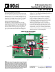


EVAL-ADP1828HC
Rev. 0 | Page 4 of 12
SOFT START
The soft start period is given by the following equation:
SSSS
tC ×= 015.8
(4)
where:
C
SS
is the soft start capacitance in microfarads.
t
SS
is the soft start period in seconds.
A C
SS
of 150 nF, which yields a 19 ms soft start period, is chosen
for this design.
CURRENT LIMIT
The external current-limit resistor can be calculated by the
following equation:
A42
mV38
2
−
⎟
⎠
⎞
⎜
⎝
⎛
Δ
+
=
DSON
L
LIMIT
CL
R
I
I
R
(5)
where:
I
LIMIT
is the output limit current.
∆I
L
is the ripple current in the inductor.
R
DSON
is the on resistance of the low-side MOSFET.
−38 mV is the CSL threshold voltage.
∆I
L
can be approximated by
Lf
DV
I
SW
OUT
L
×
−
=Δ
)1(
(6)
where:
D is the duty cycle.
L is the inductance of the inductor.
In this design, R
DSON
of the MOSFET BSC030N03LS is 4.7 mΩ
at a V
GS
of 4.5 V. Two BSC030N03LS MOSFETs in parallel yields
an effective R
DSON
of 2.35 mΩ. Because L is chosen to be 0.82 µH,
∆I
L
is calculated to be 6.6 A with a V
IN
of 18 V. If I
LIMIT
is set to
25 A, R
CL
is calculated to be 1.33 kΩ. Keep in mind that the R
DSON
of the MOSFET can vary by more than 25% from part to part,
and by more than 50% over the temperature range; therefore,
the actual current limit can vary by more than 50% from part to
part over the temperature range. For more information on this
topic or if accurate current-limit sensing is needed, see the
ADP1828 data sheet.
SWITCHING NOISE AND OVERSHOOT REDUCTION
An RC snubber can be added between SW and PGND to reduce
noise and ringing at the SW node and at the drains of the external
MOSFETs. In this design, an RC snubber is added with an R
SNUB
of 3.01 Ω and a C
SNUB
of 1.2 nF. Gate resistors can be added to
reduce overshoot voltage at the drains of the MOSFETs. For
more information, see the ADP1828 data sheet.
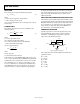
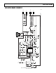
COMPENSATION DESIGN
Type III compensation is used in this design because each of
the output POSCAP capacitors has a low ESR of 5 mΩ. For
information on calculating the compensation component
values, refer to the ADP1828 data sheet.
C
HF
C
I
R
Z
C
FF
R
TOP
R
BOT
V
OUT
INTERNAL
VREF
FB
EA
COMP
R
FF
06903-002
Figure 2. Type III Compensation
The compensation values for this evaluation board have been
optimized as follows:
R
FF
= 7.5 kΩ
C
FF
= 680 pF
R
Z
= 20 kΩ
C
I
= 5.6 nF
C
HF
= 33 pF
R
TOP
= 20 kΩ
R
BOT
= 10 kΩ