
Datasheet
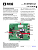


EVAL-ADP1828HC
Rev. 0 | Page 7 of 12
EVALUATION BOARD OPERATING INSTRUCTIONS
1. Connect Jumper JP3 to the on position to enable the ADP1828.
2.
Do not connect Jumper J7 (V
IN
to VREG).
3.
Connect Jumper JP2 (FREQ) to the 300 kHz position.
4.
Connect Jumper J11 (SYNC) to GND (that is, if SYNC is not used). If SYNC is used, connect SYNC to an external clock or CLKOUT
from another ADP1828.
5.
Connect Jumper JP1 (CLKSET) to high, which sets CLKOUT to 2× the internal oscillator frequency and in phase with the oscillator,
or to low, which sets CLKOUT to 1× the oscillator frequency and 180
o
out of phase.
6.
Connect the positive terminal of the input power supply to the input terminal, J8.
7.
Connect the load to the V
OUT
terminal, J13.
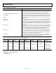
Table 1. Jumper Descriptions
Jumper Description Function
JP1 CLKSET. Clock set input.
CLKSET = high sets CLKOUT to 2 × f
OSC
CLKSET = low sets CLKOUT to 1 × f
OSC
JP2 Frequency selection. Connect to VREG for f
SW
= 600 kHz. VREG: f
SW
= 600 kHz
GND: f
SW
= 300 kHz
JP3 EN. Connect to the on position to enable the ADP1828.
EN = on enables ADP1828
EN = off disables ADP1828
J7 VREG to V
IN
. Do not connect this jumper when V
IN
is more than 5.5 V. Short VREG to V
IN
when V
IN
is less than 5.5 V
J11
SYNC. Connect SYNC to GND if the SYNC function is not used. If SYNC is used,
connect SYNC to an external clock or to the CLKOUT from another ADP1828.
Synchronization
J9
12 V supply from the disk drive connector. Short this jumper if the 12 V input supply
comes from the disk drive connector. Do not short J9 and J10 at the same time.
12 V supply from disk drive
J10
5 V supply from the disk drive connector. Short this jumper if the 5 V input supply
comes from the disk drive connector. Do not short J9 and J10 at the same time.
5 V supply from disk drive
Table 2. Evaluation Board Operating Conditions
Parameter Condition
V
IN
Input range 10 V to 18 V.
V
OUT
V
OUT
= 1.8 V at 20 A.
f
SW
Switching frequency is set to 300 kHz.
Maximum Step Load 0 A to 20 A. This design can handle a 0 A to 20 A step load at the output.
Table 3. Temperature of the Power Components
1, 2
ADP1828
Inductor
(Würth Elektronik, 744355182)
High-Side MOSFET
(Infineon Technologies, BSC080N03LS)
Low-Side MOSFETs
(Infineon Technologies, 2 × BSC030N03LS)
61°C 65°C 87°C 76°C
1
After the evaluation board ran for 30 minutes at a 20 A load, the surface temperatures of the power components were measured with an infrared thermometer.
2
V
IN
= 12 V, T
A
= 25°C