
Datasheet


EVAL-ADP1828HC
Rev. 0 | Page 8 of 12
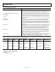
Table 4. Miscellaneous Information
Parameter Comment
Switching Frequency, f
SW
The switching frequency, f
SW
, is set to 300 kHz (Jumper JP2) on the evaluation board.
If a different f
SW
is desired, the compensation and the power components need to be
recalculated. If a f
SW
other than 300 kHz or 600 kHz is desired, a resistor, R13, can be
soldered onto the PCB to select any frequency between 300 kHz and 600 kHz.
Power MOSFETs: PG-TDSON-8 (Super-SO8) or
PowerPAK SO-8
The footprint for the power MOSFETs is laid out to fit both the PowerPAK SO-8 and the
standard SO-8 package. The board is laid out to fit two MOSFETs for the top side and two
for the bottom side. Only one high-side MOSFET is fitted on the evaluation board.
Inductor
The footprint for the inductor is laid out to fit inductors smaller or larger than the on-
board inductor.
VREG and V
IN
For input voltages less than 5.5 V, the user can connect Jumper J7 by shorting VREG to V
IN
.
Snubber Circuit
A snubber RC circuit, R
SNUB
and C
SNUB
, is laid out on the evaluation board to help
reduce switching noise and ringing at the SW node. The user can remove this RC
snubber or try different RC values for a particular application. Note that the RC snubber
dissipates power and slightly reduces the overall efficiency, generally in the range of
0.1% to 0.5%.
Gate Resistors
The dummy 0 Ω gate resistors, R2, R3, R14, and R15, are provided on the evaluation
board for reducing overshoot voltage at the drains of the external MOSFETs. The user
can change these 0 Ω resistors to different values (generally in the range of 1 Ω to
5 Ω) to achieve the desired reduction in overshoot voltage. Keep in mind that the
gate resistor dissipates power and slightly reduces the overall efficiency.
Capacitor C22
A ceramic capacitor, C22, is placed very close to the drain of the high-side MOSFET.
This capacitor, typically 0.1 μF to 1 μF, helps reduce input impedance during high
frequency transients. C22 is not assembled on the evaluation board. The user can
add this capacitor if needed for a particular application.
Voltage Divider
If a different output voltage other than 1.8 V is desired, the user needs to change the
voltage feedback divider, R7 and R8, and rework the compensation component
values as well as possibly the input and output capacitances.
Table 5. Suggestions of Power Components for Other Configurations
V
IN
Range
V
OUT
Range
Output
Current
Inductor
High-Side
MOSFETs
1
Low-Side
MOSFETs
1
Input
Capacitors
2
Output
Capacitors
3
6 V to 18 V 1.2 V to 5 V 8 A to 13 A
1 μH
4
HC7-1R0-R
BSC080N03LS BSC030N03LS 2 × 20SP180M
2R5TPD1000M5
+ 22 μF/6.3 V/X5R
6 V to 18 V 1.2 V to 5 V 13 A to 22 A
0.82 μH
5
744355182
BSC080N03LS
2 ×
BSC030N03LS
2 × 20SP180M
2 ×
2R5TPD1000M5
+ 47 μF/6.3 V/X5R
6 V to 18 V 1.2 V to 5 V 22 A to 27 A
0.47 μH
5
744355147
2 ×
BSC080N03LS
2 ×
BSC030N03LS
3 × 20SP180M
3 ×
2R5TPD1000M5
+ 47 μF/6.3 V/X5R
1
MOSFETS are from Infineon Technologies.
2
Input capacitors are the OS-CON type from Sanyo.
3
Output capacitors are the POSCAP type from Sanyo.
4
From Coiltronics.
5
From Würth Elektronik Group.