
Datasheet


ADP1870/ADP1871 Data Sheet
Rev. B | Page 2 of 44
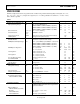
TABLE OF CONTENTS
Features .............................................................................................. 1
Applications ....................................................................................... 1
General Description ......................................................................... 1
Typical Applications Circuit ............................................................ 1
Revision History ............................................................................... 2
Specifications ..................................................................................... 3
Absolute Maximum Ratings ............................................................ 5
Thermal Resistance ...................................................................... 5
Boundary Condition .................................................................... 5
ESD Caution .................................................................................. 5
Pin Configuration and Function Descriptions ............................. 6
Typical Performance Characteristics ............................................. 7
ADP1870/ADP1871 Block Diagram ............................................ 18
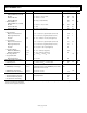
Theory of Operation ...................................................................... 19
Startup .......................................................................................... 19
Soft Start ...................................................................................... 19
Precision Enable Circuitry ........................................................ 19
Undervoltage Lockout ............................................................... 19
On-Board Low Dropout Regulator .......................................... 19
Thermal Shutdown ..................................................................... 20
Programming Resistor (RES) Detect Circuit .......................... 20
Valley Current-Limit Setting .................................................... 20
Hiccup Mode During Short Circuit ......................................... 21
Synchronous Rectifier ................................................................ 22
Power Saving Mode (PSM) Version (ADP1871).................... 22
Timer Operation ........................................................................ 22
Pseudo-Fixed Frequency ........................................................... 23
Applications Information .............................................................. 24
Feedback Resistor Divider ........................................................ 24
Inductor Selection ...................................................................... 24
Output Ripple Voltage (ΔV
RR
) .................................................. 24
Output Capacitor Selection....................................................... 24
Compensation Network ............................................................ 25
Efficiency Considerations ......................................................... 26
Input Capacitor Selection .......................................................... 27
Thermal Considerations ............................................................ 28
Design Example .......................................................................... 29
External Component Recommendations .................................... 31
Layout Considerations ................................................................... 33
IC Section (Left Side of Evaluation Board) ............................. 37
Power Section ............................................................................. 37
Differential Sensing .................................................................... 38
Typical Applications Circuits ........................................................ 39
15 A, 300 kHz High Current Application Circuit .................. 39
5.5 V Input, 600 kHz Application Circuit ............................... 39
300 kHz High Current Application Circuit ............................ 40
Outline Dimensions ....................................................................... 41
Ordering Guide .......................................................................... 42
REVISION HISTORY
7/12—Rev. A to Rev. B
Changed R
ON
= 15 mΩ/100 kΩ Valley Current Level Value from
7.5 to 3.87; Table 7 .......................................................................... 21
Updated Outline Dimensions ................................................................. 41
6/10—Rev. 0 to Rev. A
Added LFCSP Package ....................................................... Universal
Changes to Applications Section .................................................... 1
Changes to Internal Regulator Characteristics Parameter,
Table 1 ............................................................................................ 3
Changes to Table 2 and Table 3........................................................ 5
Changes to Figure 3 and Table 4 ...................................................... 6
Change to Figure 22 ....................................................................... 10
Changes to Figure 65 ...................................................................... 18
Changes to Efficiency Considerations Section ........................... 26
Changes to Table 9 ..................................................................................... 28
Added Figure 84; Renumbered Sequentially....................................... 28
Added Figure 96 ......................................................................................... 41
Changes to Ordering Guide .................................................................... 42
3/10—Revision 0: Initial Version