
Datasheet


Data Sheet ADP1870/ADP1871
Rev. B | Page 5 of 44
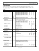
ABSOLUTE MAXIMUM RATINGS
Table 2.
Parameter Rating
VREG to PGND, GND −0.3 V to +6 V
VIN to PGND −0.3 V to +28 V
FB, COMP/EN to GND −0.3 V to (V
REG
+ 0.3 V)
DRVL to PGND −0.3 V to (V
REG
+ 0.3 V)
SW to PGND −2.0 V to +28 V
BST to SW −0.6 V to (V
REG
+ 0.3 V)
BST to PGND −0.3 V to 28 V
DRVH to SW
−0.3 V to V
REG
PGND to GND
±0.3 V
θ
JA
(10-Lead MSOP)
2-Layer Board 213.1°C/W
4-Layer Board 171.7°C/W
θ
JA
(10-Lead LFCSP)
4-Layer Board 40°C/W
Operating Junction Temperature
Range
−40°C to +125°C
Storage Temperature Range −65°C to +150°C
Soldering Conditions
JEDEC J-STD-020
Maximum Soldering Lead
Temperature (10 sec)
300°C
Stresses above those listed under Absolute Maximum Ratings
may cause permanent damage to the device. This is a stress
rating only; functional operation of the device at these or any
other conditions above those indicated in the operational
section of this specification is not implied. Exposure to absolute
maximum rating conditions for extended periods may affect
device reliability.
Absolute maximum ratings apply individually only, not in
combination. Unless otherwise specified, all other voltages are
referenced to PGND.
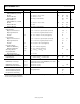
THERMAL RESISTANCE
θ
JA
is specified for the worst-case conditions, that is, a device
soldered in a circuit board for surface-mount packages.
Table 3. Thermal Resistance
Package Type θ
JA
1
Unit
θ
JA
(10-Lead MSOP)
2-Layer Board 213.1 °C/W
4- Layer Board
171.7
°C/W
θ
JA
(10-Lead LFCSP)
4- Layer Board 40 °C/W
1
θ
JA
is specified for the worst-case conditions; that is, θ
JA
is specified for the
device soldered in a circuit board for surface-mount packages.
BOUNDARY CONDITION
In determining the values given in Table 2 and Table 3, natural
convection was used to transfer heat to a 4-layer evaluation board.
ESD CAUTION