
Datasheet


ADP1870/ADP1871 Data Sheet
Rev. B | Page 6 of 44
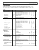
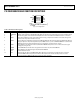
PIN CONFIGURATION AND FUNCTION DESCRIPTIONS
VIN
1
COMP/EN
2
FB
3
GND
4
VREG
5
BST
10
SW
9
DRVH
8
PGND
7
DRVL
6
ADP1870/
ADP1871
TOP VIEW
(Not to Scale)
08730-003
NOTES
1. THE EXPOSED PAD MUST BE CONNECTED
TO GROUND.
Figure 3. Pin Configuration
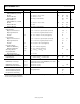
Table 4. Pin Function Descriptions
Pin No.
Mnemonic
Description
1 VIN High Input Voltage. Connect VIN to the drain of the upper-side MOSFET.
2 COMP/EN Output of the Internal Error Amplifier/IC Enable. When this pin functions as EN, applying 0 V to this pin disables the IC.
3 FB Noninverting Input of the Internal Error Amplifier. This is the node where the feedback resistor is connected.
4 GND Analog Ground Reference Pin of the IC. All sensitive analog components should be connected to this ground
plane (see the Layout Considerations section).
5 VREG Internal Regulator Supply Bias Voltage for the ADP1870/ADP1871 Controller (Includes the Output Gate Drivers).
A bypass capacitor of 1 µF directly from this pin to PGND and a 0.1 µF across VREG and GND are recommended.
VREG should not be loaded externally because it is intended to only bias internal circuitry.
6 DRVL Drive Output for the External Lower-Side, N-Channel MOSFET. This pin also serves as the current-sense gain
setting pin (see Figure 69).
7 PGND Power GND. Ground for the lower-side gate driver and lower-side, N-channel MOSFET.
8 DRVH Drive Output for the External Upper-Side, N-Channel MOSFET.
9 SW Switch Node Connection.
10 BST Bootstrap for the Upper-Side MOSFET Gate Drive Circuitry. An internal boot rectifier (diode) is connected
between VREG and BST. A capacitor from BST to SW is required. An external Schottky diode can also be
connected between VREG and BST for increased gate drive capability.