
Datasheet


Data Sheet ADP2302/ADP2303
Rev. A | Page 3 of 28
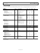
SPECIFICATIONS
V
IN
= 3.3 V, T
J
= −40°C to +125°C for minimum/maximum specifications, and T
A
= 25°C for typical specifications, unless otherwise noted.
Table 1.
Parameters Symbol Test Conditions Min Typ Max Unit
VIN
Voltage Range V
IN
3.0 20 V
Supply Current I
VIN
No switching, V
IN
= 12 V 720 950 µA
Shutdown Current I
SHDN
V
EN
= 0 V, V
IN
= 12 V 24 45 µA
Undervoltage Lockout Threshold UVLO V
IN
rising 2.7 2.9 V
V
IN
falling 2.2 2.4 V
FB
Regulation Voltage V
FB
ADP230xARDZ (adjustable) 0.788 0.8 0.812 V
ADP230xARDZ-2.5 2.463 2.5 2.538 V
ADP230xARDZ-3.3 3.25 3.3 3.35 V
ADP230xARDZ-5.0 4.925 5.0 5.075 V
Bias Current I
FB
ADP230xARDZ (adjustable) 0.01 0.1 µA
SW
On Resistance
1
V
BST
− V
SW
= 5 V, I
SW
= 200 mA 80 120 160 mΩ
Peak Current Limit ADP2302, V
BST
− V
SW
= 5 V 2.7 3.5 4.4 A
ADP2303, V
BST
− V
SW
= 5 V 4.6 5.5 6.4 A
Leakage Current V
EN
= V
SW
= 0 V, V
IN
= 12 V 0.1 5 µA
Minimum On Time 126 170 ns
Minimum Off Time 210 280 ns
OSCILLATOR FREQUENCY f
SW
595 700 805 kHz
SOFT START TIME 2048 Clock cycles
EN
Input Threshold V
EN
1.12 1.2 1.28 V
Input Hysteresis 100 mV
Pull-Down Current 1.2 µA
BOOTSTRAP VOLTAGE V
BOOT
V
IN
= 12 V 4.7 5.0 5.3 V
PGOOD
PGOOD Rising Threshold 82.5 87.5 92.5 %
PGOOD Hysteresis 2.5 %
PGOOD Deglitch Time
2
32 Clock cycles
PGOOD Output Low Voltage 150 300 mV
PGOOD Leakage Current V
PGOOD
= 5 V 0.1 1 µA
THERMAL SHUTDOWN
Threshold Rising temperature 150 °C
Hysteresis 15 °C
1
Pin-to-Pin measurements.
2
Guaranteed by design.