
Datasheet


ADP2302/ADP2303 Data Sheet
Rev. A | Page 4 of 28
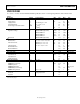
ABSOLUTE MAXIMUM RATINGS
Table 2.
Parameter MAX Rating
VIN, EN, PGOOD −0.3 V to +24 V
SW −1.0 V to +24 V
BST to SW −0.6 V to +6 V
FB, NC −0.3 V to +6 V
Operating Junction Temperature Range −40°C to +125°C
Storage Temperature Range −65°C to +150°C
Soldering Conditions JEDEC J-STD-020
Stresses above those listed under Absolute Maximum Ratings
may cause permanent damage to the device. This is a stress
rating only; functional operation of the device at these or any
other conditions above those indicated in the operational
section of this specification is not implied. Exposure to absolute
maximum rating conditions for extended periods may affect
device reliability.
Absolute maximum ratings apply individually only, not in
combination. Unless otherwise specified, all voltages are
referenced to GND.
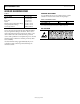
THERMAL RESISTANCE
θ
JA
is specified for the worst-case conditions, that is, a device
soldered in a circuit board for surface-mount packages.
Table 3. Thermal Resistance
1
Package Type θ
JA
Unit
8-Lead SOIC_N_EP 58.5 °C/W
1
JA
is measured using natural convection on JEDEC 4-layer board.
ESD CAUTION