
Datasheet

Data Sheet ADP2302/ADP2303
Rev. A | Page 5 of 28
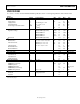
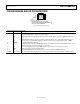
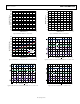
PIN CONFIGURATION AND FUNCTION DESCRIPTIONS
BST 1
VIN 2
EN
3
PGOOD 4
SW8
GND7
NC
6
FB5
NOTES
1. NC = NO CONNECT.
2. THE EXPOSED PAD SHOULD BE SOLDERED
TO AN EXTERNAL GROUND PLANE UNDERNE ATH
THE IC FOR THERMAL DISSIPATION.
ADP2302
ADP2303
TOP VIEW
(Not to Scale)
08833-003
Figure 3. Pin Configuration (Top View)
Table 4. Pin Function Descriptions
Pin No. Mnemonic Description
1 BST
Bootstrap Supply for the High-Side MOSFET Driver. A 0.1 µF capacitor is connected between SW and BST to
provide a floating driver voltage for the power switch.
2 VIN
Power Input. Connect to the input power source with a ceramic bypass capacitor to GND directly from this
pin.
3 EN
Output Enable. Pull this pin high to enable the output. Pull this pin low to disable the output. This pin can
also be used as a programmable UVLO input. This pin has an internal 1.2 µA pull-down current to GND.
4 PGOOD Power-Good Open-Drain Output.
5 FB
Feedback Voltage Sense Input. For the adjustable version, connect this pin to a resistive divider from V
OUT
. For
the fixed output version, connect this pin to V
OUT
directly.
6 NC Used for internal testing. Connect to GND or leave this pin floating to ensure proper operation.
7 GND Ground. Connect this pin to the ground plane.
8 SW Switch Node Output. Connect an inductor to V
OUT
and a catch diode to GND from this pin.
9 (EPAD) Exposed Pad The exposed pad should be soldered to an external ground plane underneath the IC for thermal dissipation.