
Datasheet


ADP2370/ADP2371 Data Sheet
Rev. C | Page 2 of 32
TABLE OF CONTENTS
Features .............................................................................................. 1
Applications ....................................................................................... 1
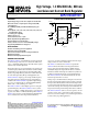
Typical Application Circuit ............................................................. 1
General Description ......................................................................... 1
Revision History ............................................................................... 2
Specifications ..................................................................................... 3
Recommended Specifications: Capacitors ................................ 5
Absolute Maximum Ratings ....................................................... 6
Thermal Data ................................................................................ 6
Thermal Resistance ...................................................................... 6
ESD Caution .................................................................................. 6
Pin Configuration and Function Descriptions ............................. 7
Typical Performance Characteristics ............................................. 8
Buck Output .................................................................................. 8
Theory of Operation ...................................................................... 20
PWM Operation ......................................................................... 20
PSM Operation ........................................................................... 21
Features Descriptions ..................................................................... 22
Precision Enable ......................................................................... 22
Forced PWM or PWM/PSM Selection.................................... 22
Quick Output Discharge (QOD) Function ............................. 22
Short-Circuit Protection ............................................................ 22
Undervoltage Lockout ............................................................... 22
Thermal Protection .................................................................... 22
Soft Start ...................................................................................... 22
Current Limit .............................................................................. 22
100% Duty Cycle ........................................................................ 23
Synchronizing ............................................................................. 23
Power Good ................................................................................ 24
Applications Information .............................................................. 25
ADIsimPower Design Tool ....................................................... 25
External Component Selection ................................................ 25
Selecting the Inductor ................................................................ 25
Output Capacitor ........................................................................ 25
Input Capacitor ........................................................................... 25
Adjustable Output Voltage Programming .............................. 25
Efficiency ..................................................................................... 26
Recommended Buck External Components .......................... 26
Capacitor Selection .................................................................... 28
Thermal Considerations ................................................................ 29
PCB Layout Considerations ...................................................... 30
Packaging and Ordering Information ......................................... 32
Outline Dimensions ................................................................... 32
Ordering Guide .......................................................................... 32
REVISION HISTORY
11/12—Rev. B to Rev. C
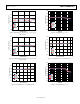
Change to Figure 6 ........................................................................... 8
Changes to Ordering Guide............................................................. 32
8/12—Rev. A to Rev. B
Change to Figure 62 ....................................................................... 17
Changes to Figure 63, Figure 64, Figure 65, and Figure 66 ............ 18
5/12—Rev. 0 to Rev. A
Changed Voltage Range for SW to PGND and Ground Plane
from −0.3 V to VIN + 0.3 V to −0.7 V to VIN + 0.3 V ............... 6
Changes to Ordering Guide .......................................................... 32
4/12—Revision 0: Initial Version