
Datasheet
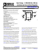


ADP2370/ADP2371 Data Sheet
Rev. C | Page 6 of 32
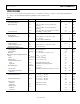
ABSOLUTE MAXIMUM RATINGS
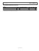
Table 3.
Parameter Rating
VIN to PGND and Ground Plane
−0.3 V to +17 V
SW to PGND and Ground Plane −0.7 V to VIN + 0.3 V
FB to PGND and Ground Plane −0.3 V to +6 V
EN to PGND and Ground Plane −0.3 V to +17 V
PG to PGND and Ground Plane −0.3 V to +17 V
SYNC to PGND and Ground Plane −0.3 V to +17 V
FSEL to PGND and Ground Plane −0.3 V to +17 V
Temperature Range
Storage −65°C to +150°C
Operating Ambient −40°C to +85°C
Operating Junction −40°C to +125°C
Soldering Conditions JEDEC J-STD-020
St
r
es
ses a
bove those listed
under Ab
so
l
ut
e M
a
xi
mum
R
at
i
ngs
m
ay cau
se p
erm
ane
nt dama
ge t
o t
h
e d
ev
i
ce
. This is a
str
e
ss
r
ati
n
g o
n
ly
; fu
n
ct
io
n
al
op
e
ra
t
io
n o
f
th
e d
evic
e at
th
e
se
or
a
ny
o
t
her co
ndi
ti
ons
ab
o
ve t
ho
s
e indi
ca
t
ed
i
n t
he
o
pe
rati
onal
se
c
ti
on
o
f t
h
is s
pe
c
ifi
ca
t
ion is
not i
mpl
ie
d.
Ex
p
osu
re
t
o a
b
so
lu
te
ma
x
im
um
r
at
in
g co
ndi
tio
ns for
ex
t
en
de
d
pe
ri
o
ds
m
ay
aff
e
ct
d
e
vic
e r
e
li
ab
i
li
t
y.
THERMAL DATA
Absolute maximum ratings apply individually only, not in com-
bination. Exceeding the junction temperature (T
J
) limit can
cause damage to the ADP2370/ADP2371. Monitoring ambient
temperature does not guarantee that T
J
is within the specified
temperature limits. The maximum ambient temperature may
require derating in applications with high power dissipation and
poor thermal resistance.
In applications with moderate power dissipation and low
printed circuit board (PCB) thermal resistance, the maximum
ambient temperature can exceed the maximum limit as long
as the junction temperature is within specification limits. The
junction temperature of the device is dependent on the ambient
temperature, the power dissipation of the device, and the junction
to ambient thermal resistance of the package (θ
JA
).
Maximum junction temperature (T
J
) is calculated from the
ambient temperature (T
A
) and power dissipation (P
D
) using
the formula
T
J
= T
A
+ (P
D
× θ
JA
)
Junction-to-ambient thermal resistance (θ
JA
) of the package
is based on modeling and calculation using a 4-layer board.
θ
JA
is highly dependent on the application and board layout. In
applications where high maximum power dissipation exists,
close attention to thermal board design is required. The value
of θ
JA
can vary, depending on PCB material, layout, and
environmental conditions.
The specified values of θ
JA
are based on a 4-layer, 4 in. × 3 in.
circuit board. See JESD 51-7, High Effective Thermal Conduc-
tivity Test Board for Leaded Surface Mount Packages, for detailed
information on board construction. For more information, see
Application Note AN-772, A Design and Manufacturing Guide for
the Lead Frame Chip Scale Package (LFCSP).
Ψ
JB
is the junction to board thermal characterization parameter
with units of °C/W. The Ψ
JB
of the package is based on modeling
and calculation using a 4-layer board. The JESD51-12, Guidelines
for Reporting and Using Electronic Package Thermal Information,
states that thermal characterization parameters are not the same
as thermal resistances. Ψ
JB
measures the component power flowing
through multiple thermal paths rather than a single path as in
thermal resistance, θ
JB
. Therefore, Ψ
JB
thermal paths include
convection from the top of the package as well as radiation
from the package, factors that make Ψ
JB
more useful in real-
world applications. Maximum junction temperature (T
J
) is
calculated from the board temperature (T
B
) and power
dissipation (P
D
) using the formula
T
J
= T
B
+ (P
D
× Ψ
JB
)
For more detailed information regarding Ψ
JB
, see JESD51-12
and JESD51-8, Integrated Circuit Thermal Test Method Envi-
ronmental Conditions—Junction-to-Board.
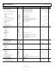
THERMAL RESISTANCE
θ
JA
and Ψ
JB
are specified for the worst-case conditions, that is, a
device soldered in a circuit board for surface-mount packages.
θ
JC
is a parameter for surface-mount packages with top mounted
heat sinks.
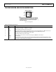
Table 4. Thermal Resistance
Package Type θ
JA
θ
JC
Ψ
JB
Unit
8-Lead 3 mm × 3 mm LFCSP 36.7 23.5 17.2 °C/W
ESD CAUTION