
Datasheet


Data Sheet ADP2370/ADP2371
Rev. C | Page 7 of 32
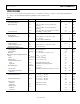
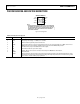
PIN CONFIGURATION AND FUNCTION DESCRIPTIONS
09531-002
ADP2370/ADP2371
TOP VIEW
(Not to
Scale)
3EN
4
SYNC
1VIN
NOTES
1. THE EXPOSED PAD ON THE BOTTOM OF THE PACKAGE ENHANCES
THE THERMAL PERFORMANCE AND IS ELECTRICALLY CONNECTED
TO GROUND INSIDE THE PACKAGE. THE EXPOSED PAD MUST BE
CONNECTED TO THE GROUND PLANE ON THE CIRCUIT BOARD
FOR PROPER OPERATION.
2FSEL
6 PG
5
FB
8
PGND
7 SW
Figure 2. Pin Configuration
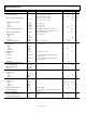
Table 5. Pin Function Descriptions
Pin No. Mnemonic Description
1
VIN
Power Input.
2 FSEL Frequency Select. High = 1.2 MHz, low = 600 kHz.
3 EN Enable. Enable input with precision thresholds.
4 SYNC Synchronize. This pin is used to synchronize the device to an external 600 kHz to 1.2 MHz clock or forces
PWM mode when it is held high. SYNC held low forces automatic PWM/PSM operation.
5 FB Feedback. This pin provides feedback from the output.
6 PG Power Good. PG is an open-drain output.
7 SW Switch. This pin serves as the connection from the power MOSFETs to the inductor.
8 PGND Power Ground.
EPAD Exposed Pad. The exposed pad on the bottom of the package enhances the thermal performance and is
electrically connected to ground inside the package. The exposed pad must be connected to the ground
plane on the circuit board for proper operation.