
Datasheet


ADP3303
–3–
REV.
CAUTION
ESD (electrostatic discharge) sensitive device. Electrostatic charges as high as 4000 V readily
accumulate on the human body and test equipment and can discharge without detection.
Although the ADP3303 features proprietary ESD protection circuitry, permanent damage may
occur on devices subjected to high energy electrostatic discharges. Therefore, proper ESD
precautions are recommended to avoid performance degradation or loss of functionality.
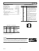
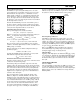
PIN FUNCTION DESCRIPTIONS
Pin Mnemonic Function
1 & 2 OUT Output of the Regulator. Bypass to
ground with a 0.47 µF or larger
capacitor. Pins 1 and 2 must be con-
nected together for proper operation.
3 NR Noise Reduction Pin. Used for reduc-
tion of the output noise. (See text for
details.) No connection if not used.
4 GND Ground Pin.
5 SD Active Low Shutdown Pin. Connect to
ground to disable the regulator output.
When shutdown is not used, this pin
should be connected to the input pin.
6 ERR Open Collector Output. Goes low to
indicate that the output is about to go
out of regulation.
7 & 8 IN Regulator Input. Pins 7 and 8 must
be connected together for proper
operation.
PIN CONFIGURATION
1
2
3
4
8
7
6
5
TOP VIEW
(Not to Scale)
OUT
OUT
NR
GND
IN
IN
ERR
SD
ADP3303
ABSOLUTE MAXIMUM RATINGS*
Input Supply Voltage . . . . . . . . . . . . . . . . . . . –0.3 V to +16 V
Shutdown Input Voltage . . . . . . . . . . . . . . . . –0.3 V to +16 V
Error Flag Output Voltage . . . . . . . . . . . . . . . –0.3 V to +16 V
Noise Bypass Pin Voltage . . . . . . . . . . . . . . . . –0.3 V to +5 V
Power Dissipation . . . . . . . . . . . . . . . . . . . Internally Limited
Operating Ambient Temperature Range . . . . – °C to +85°C
Operating Junction Temperature Range . . . – °C to +125°C
θ
JA
. . . . . . . . . . . . . . . . . . . . . . . . . . . . . . . . . . . . . 96°C/W
θ
JC
. . . . . . . . . . . . . . . . . . . . . . . . . . . . . . . . . . . . . 55°C/W
Storage Temperature Range . . . . . . . . . . . . –65°C to +150°C
Lead Temperature Range (Soldering 10 sec) . . . . . . . +300°C
Vapor Phase (60 sec) . . . . . . . . . . . . . . . . . . . . . . . +215°C
Infrared (15 sec) . . . . . . . . . . . . . . . . . . . . . . . . . . +220°C
*This is a stress rating only; operation beyond these limits can cause the device to
be permanently damaged.
Other Members of anyCAP Family
1
Output Package
Model Current Options
2
Comments
ADP3300 50 mA SOT-23-6 High Accuracy
ADP3301 100 mA SO-8 High Accuracy
ADP3302 100 mA SO-8 Dual Output
ADP3307 100 mA SOT-23-6 Small Size
ADP3308 50 mA SOT-23-5 Improved LP2980
ADP3309 100 mA SOT-23-5 Improved MIC5205
NOTES
1
See individual data sheets for detailed ordering information.
2
SO = Small Outline, SOT = Surface Mount.
WARNING!
ESD SENSITIVE DEVICE
B
25
25