
Datasheet
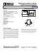
Table Of Contents

ADP3335 Data Sheet
Rev. D | Page 2 of 16
TABLE OF CONTENTS
Features .............................................................................................. 1
Applications ....................................................................................... 1
Functional Block Diagram .............................................................. 1
General Description ......................................................................... 1
Revision History ............................................................................... 2
Specifications ..................................................................................... 3
Absolute Maximum Ratings ............................................................ 4
ESD Caution .................................................................................. 4
Pin Configuration and Function Descriptions ............................. 5
Typical Performance Characteristics ............................................. 6
Theory of Operation ........................................................................ 9
Applications Information .............................................................. 10
Output Capacitor Selection ....................................................... 10
Input Bypass Capacitor .............................................................. 10
Noise Reduction ......................................................................... 10
Thermal Overload Protection .................................................. 10
Calculating Junction Temperature ........................................... 10
Printed Circuit Board Layout Considerations ....................... 11
LFCSP Layout Considerations .................................................. 11
Shutdown Mode ......................................................................... 11
Outline Dimensions ....................................................................... 12
Ordering Guide .......................................................................... 13
REVISION HISTORY
10/13—Rev. C to Rev. D
Updated Outline Dimensions ....................................................... 12
Changes to Ordering Guide .......................................................... 13
12/12—Rev. B to Rev. C
Changes to Figure 14 and Figure 16 ............................................... 7
Updated Outline Dimensions ....................................................... 12
Changes to Ordering Guide .......................................................... 13
6/10—Rev. A to Rev. B
Added Exposed Pad Notation to Figure 4 and Table 3 ................ 5
Added Exposed Pad Notation to Outline Dimensions ............. 12
Changes to Ordering Guide .......................................................... 13
1/04—Rev. 0 to Re v. A
Format Updated .................................................................. Universal
Renumbered Figures .......................................................... Universal
Removed Figure 22 ............................................................................ 6
Change to Printed Circuit Board Layout Considerations
Section .............................................................................................. 11
Added LFCSP Layout Considerations Section ........................... 11
Added Package Drawing ................................................... Universal
Changes to Ordering Guide .......................................................... 16