
Datasheet
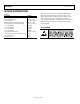
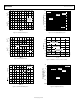
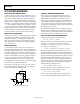
Table Of Contents

Data Sheet ADP3335
Rev. D | Page 9 of 16
THEORY OF OPERATION
The ADP3335 uses a single control loop for regulation and
reference functions. The output voltage is sensed by a resistive
voltage divider, R1 and R2, which is varied to provide the
available output voltage option. Feedback is taken from this
network by way of a series diode, D1, and a second resistor
divider, R3 and R4, to the input of an amplifier.
INPUT
00147-0-023
OUTPUT
COMPENSATION
CAPACITOR
R2
R1
GND
ADP3335
PTAT
CURRENT
R4
PTAT
V
OS
g
m
Q1
ATTENUATION
(V
BANDGAP
/V
OUT
)
R3
D1
(a)
C
LOAD
R
LOAD
NONINVERTING
WIDEBAND
DRIVER
Figure 23. Functional Block Diagram
A very high gain error amplifier is used to control this loop. The
amplifier is constructed in such a way that equilibrium produces a
large, temperature proportional input offset voltage that is
repeatable and very well controlled. The temperature proportional
offset voltage combines with the complementary diode voltage
to form a virtual band gap voltage implicit in the network, although
it never appears explicitly in the circuit.
This patented design makes it possible to control the loop with
only one amplifier. This technique also improves the noise
characteristics of the amplifier by providing more flexibility in
the trade-off of noise sources that leads to a low noise design.
The R1 and R2 divider is chosen in the same ratio as the band gap
voltage to the output voltage. Although the R1 and R2 resistor
divider is loaded by the D1 diode and a second divider—R3 and
R4, the values can be chosen to produce a temperature stable
output. This unique arrangement specifically corrects for the
loading of the divider, thus avoiding the error resulting from
base current loading in conventional circuits.
The patented amplifier controls a new and unique noninverting
driver that drives the pass transistor, Q1. This special noninverting
driver enables the frequency compensation to include the load
capacitor in a pole-splitting arrangement to achieve reduced
sensitivity to the value, type, and ESR of the load capacitance.
Most LDOs place very strict requirements on the range of ESR
values for the output capacitor, because they are difficult to
stabilize due to the uncertainty of load capacitance and resistance.
The ESR value required to keep conventional LDOs stable,
moreover, changes depending on load and temperature. These
ESR limitations make designing with LDOs more difficult
because of their unclear specifications and extreme variations
over temperature.
With the ADP3335, ESR limitations are no longer a source of
design constraints. The ADP3335 can be used with virtually any
good quality capacitor and with no constraint on the minimum
ESR. This innovative design allows the circuit to be stable with
just a small 1 µF capacitor on the output. Additional advantages
of the pole-splitting scheme include superior line noise reject-
tion and very high regulator gain, which lead to excellent line
and load regulation. Impressive ±1.8% accuracy is guaranteed
over line, load, and temperature.
Additional features of the circuit include current limit, thermal
shutdown, and noise reduction.