
Datasheet
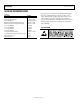
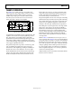

Table Of Contents

ADP3335 Data Sheet
Rev. D | Page 10 of 16
APPLICATIONS INFORMATION
OUTPUT CAPACITOR SELECTION
As with any micropower device, output transient response is a
function of the output capacitance. The ADP3335 is stable over
a wide range of capacitor values, types, and ESR (anyCAP). A
capacitor as low as 1 µF is all that is needed for stability; larger
capacitors can be used if high output current surges are anticipated.
The ADP3335 is stable with extremely low ESR capacitors (ESR
≈ 0), such as multilayer ceramic capacitors (MLCC) or organic
semiconductor electrolytic capacitors (OSCON). Note that the
effective capacitance of some capacitor types may fall below the
minimum at extreme temperatures. Ensure that the capacitor
provides more than 1 µF over the entire temperature range.
INPUT BYPASS CAPACITOR
An input bypass capacitor is not strictly required, but is advisable
in any application involving long input wires or high source
impedance. Connecting a 1 µF capacitor from IN to ground
reduces the circuit’s sensitivity to PC board layout. If a larger
value output capacitor is used, then a larger value input capacitor
is also recommended.
NOISE REDUCTION
A noise reduction capacitor (C
NR
) can be used, as shown in
Figure 24, to further reduce the noise by 6 dB to 10 dB (Figure 22).
Low leakage capacitors in the 100 pF to 1 nF range provide the best
performance. Since the noise reduction pin, NR, is internally
connected to a high impedance node, any connection to this node
should be made carefully to avoid noise pickup from external
sources. The pad connected to this pin should be as small as
possible, and long PC board traces are not recommended.
When adding a noise reduction capacitor, maintain a minimum
load current of 1 mA when not in shutdown.
It is important to note that as C
NR
increases, the turn-on time
will be delayed. With NR values greater than 1 nF, this delay
may be on the order of several milliseconds.
NR
IN
IN
OUT
OUT
OUT
GND
SD
ADP3335
ON
OFF
V
IN
C
IN
1µF
+
+
V
OUT
00147-0-021
1
3
4
7
2
5
6
8
C
OUT
1µF
C
NR
Figure 24. Typical Application Circuit
THERMAL OVERLOAD PROTECTION
The ADP3335 is protected against damage from excessive
power dissipation by its thermal overload protection circuit,
which limits the die temperature to a maximum of 165°C.
Under extreme conditions (i.e., high ambient temperature and
power dissipation) where die temperature starts to rise above
165°C, the output current is reduced until the die temperature
has dropped to a safe level. The output current is restored when
the die temperature is reduced.
Current and thermal limit protections are intended to protect
the device against accidental overload conditions. For normal
operation, device power dissipation should be externally limited
so that junction temperatures will not exceed 150°C.
CALCULATING JUNCTION TEMPERATURE
Device power dissipation is calculated as follows:
P
D
= (V
IN
− V
OUT
)I
LOAD
+ (V
IN
)I
GND
Where I
LOAD
and I
GND
are load current and ground current, and
V
IN
and V
OUT
are input and output voltages, respectively.
Assuming I
LOAD
= 400 mA, I
GND
= 4 mA, V
IN
= 5.0 V, and V
OUT
=
3.3 V, device power dissipation is
P
D
= (5 V – 3.3 V)400 mA + 5.0 V(4 mA) = 700 mW
The junction temperature can be calculated from the power
dissipation, ambient temperature, and package thermal resistance.
The thermal resistance is a function not only of the package, but
also of the circuit board layout. Standard test conditions are used to
determine the values published in this data sheet, but actual
performance will vary. For an LFCSP-8 package mounted on a
standard 4-layer board, θ
JA
is 48°C/W. In the above example, where
the power dissipation is 700 mW, the temperature rise above
ambient will be approximately equal to
∆T
JA
= 0.700 W × 48°C/W = 33.6°C
To limit the maximum junction temperature to 150°C, the
maximum allowable ambient temperature will be
T
AMAX
= 150°C − 33.6°C = 116.4°C
In this case, the resulting ambient temperature limitation is
above the maximum allowable ambient temperature of 85°C.