
Datasheet
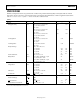
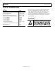
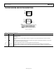
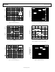
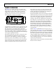

Table Of Contents

Data Sheet ADP3335
Rev. D | Page 5 of 16
PIN CONFIGURATION AND FUNCTION DESCRIPTIONS
ADP3335
TOP VIEW
(Not to Scale)
OUT
1
OUT
2
OUT
3
GND
4
IN
IN
SD
NR
8
7
6
5
00147-0-022
Figure 3. 8-Lead MSOP
S
D
1
2
3
4
7
8
6
5
T
OP
V
IE
W
(Not to
S
ca
le
)
O
UT
OUT
G
ND
I
N
I
N
NR
AD
P
33
35
OUT
00147-0-025
N
OT
E
S
1
. T
H
E E
XP
OS
ED
PA
D
ON
TH
E
BO
T
TO
M O
F
TH
E P
A
CK
AG
E
E
NHA
NCE
S TH
E TH
ERM
AL P
ERF
ORMA
NCE
AN
D IS
ELECTRICALLY CONNECTED TO DIE SUBSTRATE.
THERMAL VIAS MUST BE ISOLATED OR CONNECTED
TO IN. DO NOT CONNECT THE THERMAL PAD TO
GROUND.
Figure 4. 8-Lead LFCSP
Table 3. Pin Function Descriptions
Pin No.
Mnemonic
Function
1, 2, 3 OUT
Output of the Regulator. Bypass to ground with a 1.0 µF or larger capacitor. All pins must be connected together
for proper operation.
4 GND Ground Pin.
5 NR
Noise Reduction Pin. Used for further reduction of output noise (see the Noise Reduction section for further
details).
6
SD
Active Low Shutdown Pin. Connect to ground to disable the regulator output. When shutdown is not used, this
pin should be connected to the input pin.
7, 8
IN
Regulator Input. All pins must be connected together for proper operation.
EP
Exposed
Pad
The exposed pad on the bottom of the LFCSP package enhances thermal performance and is electrically
connected to the die substrate, which is electrically common with the input pins, IN (Pin 7 and Pin 8), inside the
package.