
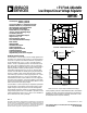
Datasheet


REV. 0
Information furnished by Analog Devices is believed to be accurate and
reliable. However, no responsibility is assumed by Analog Devices for its
use, nor for any infringements of patents or other rights of third parties
which may result from its use. No license is granted by implication or
otherwise under any patent or patent rights of Analog Devices.
a
ADP3367
© Analog Devices, Inc., 1995
One Technology Way, P.O. Box 9106, Norwood, MA 02062-9106, U.S.A.
Tel: 617/329-4700 Fax: 617/326-8703
+5 V Fixed, Adjustable
Low-Dropout Linear Voltage Regulator
FEATURES
Low Dropout: 150 mV @ 200 mA
Low Dropout: 300 mV @ 300 mA
Low Power CMOS: 17 mA Quiescent Current
Shutdown Mode: 0.2 mA Quiescent Current
300 mA Output Current Guaranteed
Pin Compatible with MAX667
Stable with 10 mF Load Capacitor
+2.5 V to +16.5 V Operating Range
Low Battery Detector
Fixed +5 V or Adjustable Output
High Accuracy: 62%
Dropout Detector Output
Low Thermal Resistance Package*
ESD > 6000 V
APPLICATIONS
Handheld Instruments
Cellular Telephones
Battery Operated Devices
Portable Equipment
Solar Powered Instruments
High Efficiency Linear Power Supplies
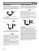
FUNCTIONAL BLOCK DIAGRAM
ADP3367
IN
SHDN
LBO
LBI
GND
50mV
SET
DD
OUT
1.255V
REF
A1
C1
C2
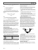
TYPICAL OPERATING CIRCUIT
IN
OUT
GNDSET SHDN
ADP3367
+5V
OUTPUT
C1
10µF
+
+
+6V
INPUT
V
IN
–V
OUT
– V
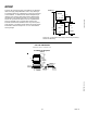
400
200
0
015
LOAD CURRENT – mA
510
100
T
A
= +50°C
300
GUARANTEED 300mA
ADP3367
DISSIPATION LIMIT
STANDARD
SO PACKAGE
DISSIPATION LIMIT
Load Current vs. Input-Output Differential Voltage
ADI’s proprietary Thermal Coastline leadframe used in ADP3367AR
packaging, has 30% lower thermal resistance than the standard
leadframes. This improvement in heat flow rate results in lower
die temperature hence improves reliability.
GENERAL DESCRIPTION
The ADP3367 is a low-dropout precision voltage regulator that
can supply up to 300 mA output current. It can be used to give
a fixed +5 V output with no additional external components or
can be adjusted from +1.3 V to +16 V using two external
resistors. Fixed or adjustable operation can be selected via the
SET input. The low quiescent current (17 µA) in conjunction
with the standby or shutdown mode (0.2 µA) makes this device
especially suitable for battery powered systems. The dropout
voltage when supplying 100 µA is only 15 mV allowing opera-
tion with minimal headroom thereby prolonging the useful bat-
tery life. At higher output current levels the dropout remains
low increasing to just 150 mV when supplying 200 mA. A wide
input voltage range from 2.5 V to 16.5 V is allowable. Addi-
tional features include a dropout detector and a low supply/bat-
tery monitoring comparator. The dropout detector can be used
to signal loss of regulation while the low battery detector can be
used to monitor the input supply voltage.
The ADP3367 is a much improved pin-compatible replacement
for the MAX667. Improvements include lower supply current,
tighter voltage accuracy and superior line and load regulation.
Improved ESD protection (>6000 V) is achieved by advanced
voltage clamping structures. The ADP3367 is specified over the
industrial temperature range –40°C to +85°C and is available in
narrow surface mount (SOIC) packages.