
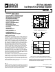
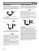
Datasheet
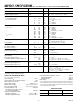


ADP3367–SPECIFICATIONS
Parameter Min Typ Max Units Test Conditions/Comments
Input Voltage, V
IN
2.5 16.5 V
Output Voltage, V
OUT
4.9 5.0 5.1 V V
SET
= 0 V, V
IN
= 6 V, I
OUT
= 10 mA
Maximum Output Current 200 mA V
IN
= +9 V, + 4.5 V < V
OUT
< +5.5 V
Quiescent Current
I
GND
: Shutdown Mode 0.2 0.75 µAV
SHDN
= 2 V
I
GND
: Normal Mode V
SHDN
= 0 V, V
SET
= 0 V
17 25 µAI
OUT
= 0 µA
20 30 µAI
OUT
= 100 µA
514 mAI
OUT
= 200 mA
Dropout Voltage
V
OUT
= 5 V 15 40 mV I
OUT
= 100 µA
60 125 mV I
OUT
= 50 mA
100 175 mV I
OUT
= 100 mA
150 250 mV I
OUT
= 200 mA, T
A
= +25°C
175 300 mV I
OUT
= 200 mA
300 500 mV I
OUT
= 300 mA
V
OUT
= 3.3 V 94 140 mV I
OUT
= 50 mA
210 312 mV I
OUT
= 100 mA
430 625 mV I
OUT
= 200 mA, T
A
= +25°C
Load Regulation 5 10 mV I
OUT
= 10 mA–100 mA, V
IN
= 6 V
I
OUT
= 10 mA–200 mA, V
IN
= 6 V
Line Regulation 0.1 5 mV V
IN
= 6 V to 10 V, I
OUT
= 10 mA
Reference Voltage, V
SET
1.23 1.255 1.28 V
SET Input Threshold 50 mV
SET Input Current, I
SET
±0.01 ±10 nA V
SET
= 1.5 V
Output Leakage Current, I
OUT
0.1 1 µAV
SHDN
= 2 V
Short Circuit Current, I
OUT
400 mA T
A
= +25°C
450 mA T
A
= T
MIN
to T
MAX
Low Battery Detector Input Threshold, V
LBI
1.215 1.255 1.295 V
LBI Hysteresis 6 mV
LBI Input Leakage Current, I
LBI
±0.01 ±10 nA V
LBI
= 1.5 V
Low Battery Detector Output Voltage, V
LBO
0.25 V V
LBI
= 0 V, I
LBO
= 10 mA, T
A
= +25°C
0.40 V V
LBI
= 0 V, I
LBO
= 10 mA, T
A
= T
MIN
to T
MAX
Shutdown Input Voltage, V
SHDN
1.5 V V
IH
0.4 V V
IL
Shutdown Input Current, I
SHDN
±0.01 ±10 nA V
SHDN
= 0 V to V
IN
Dropout Detector Output Voltage 0.25 V (V
SET
= 0 V, V
SHDN
= 0 V, R
DD
= 100 kΩ,
V
IN
= 7 V, I
OUT
= 10 mA)
4.0 (V
SET
= 0 V, V
SHDN
= 0 V, R
DD
= 100 kΩ,
V
IN
= 4.5 V, I
OUT
= 10 mA)
Specifications subject to change without notice.
(V
IN
= +9 V, GND = 0 V, V
OUT
= +5 V, T
A
= T
MIN
to T
MAX
unless otherwise noted)
–2–
REV. 0
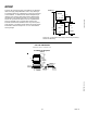
ORDERING GUIDE
Model Temperature Range Package Option*
ADP3367AR –40°C to +85°C SO-8
*SO = Small Outline Package.
ABSOLUTE MAXIMUM RATINGS*
(
T
A
= +25°C unless otherwise noted)
Input Voltage, V
IN
. . . . . . . . . . . . . . . . . . . . . . . . . . . . . +18 V
Output Short Circuit to GND Duration . . . . . . . . . . . . . 1 sec
LBO Output Sink Current . . . . . . . . . . . . . . . . . . . . . . . 50 mA
LBO Output Voltage . . . . . . . . . . . . . . . . . . . . . GND to V
OUT
SHDN Input Voltage . . . . . . . . . . . . . . –0.3 V to (V
IN
+ 0.3 V)
LBI, SET Input Voltage . . . . . . . . . . . –0.3 V to (V
IN
+ 0.3 V)
Power Dissipation, R-8 . . . . . . . . . . . . . . . . . . . . . . . 960 mW
(Derate 10 mW/°C above +50°C)
θ
JA
, Thermal Impedance . . . . . . . . . . . . . . . . . . . . . . 98°C/W
Operating Temperature Range
Industrial (A Version) . . . . . . . . . . . . . . . . . –40°C to +85°C
Storage Temperature Range . . . . . . . . . . . –65°C to +150°C
Lead Temperature (Soldering, 10 sec) . . . . . . . . . . . . . +300°C
Vapor Phase (60 sec) . . . . . . . . . . . . . . . . . . . . . . . . +215°C
Infrared (15 sec) . . . . . . . . . . . . . . . . . . . . . . . . . . . . +220°C
ESD Rating . . . . . . . . . . . . . . . . . . . . . . . . . . . . . . . . > 6000 V
*This is a stress rating only and functional operation of the device at these or any
other conditions above those indicated in the operation sections of this specifica-
tion is not implied. Exposure to absolute maximum rating conditions for extended
periods of time may affect reliability.