
Datasheet


ADP3367
REV. 0
–3–
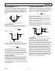
PIN FUNCTION DESCRIPTION
Mnemonic Function
DD Dropout Detector Output. PNP collector output
which sources current as dropout is reached.
V
IN
Voltage Regulator Input.
GND Ground Pin. Must be connected to 0 V.
LBI Low Battery Detect Input. Compared with 1.255 V.
LBO Low Battery Detect Output. Open Drain Output
that goes low when LBI is below the threshold.
SHDN Digital Input. May be used to disable the device
so that the power consumption is minimized.
SET Voltage Setting Input. Connect to GND for +5 V
output or connect to resistive divider for adjust-
able output.
OUT Regulated Output Voltage. Connect to filter
capacitor.
DIP & SOIC PIN CONFIGURATION
DD
OUT
LBI
GND
IN
LBO
SET
SHDN
1
2
3
4
8
7
6
5
TOP VIEW
(Not to Scale)
ADP3367
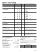
TERMINOLOGY
Dropout Voltage: The input/output voltage differential at
which the regulator no longer maintains regulation against fur-
ther reductions in input voltage. It is measured when the output
decreases 100 mV from its nominal value. The nominal value is
the measured value with V
IN
= V
OUT
+2 V.
Line Regulation: The change in output voltage as a result of a
change in the input voltage. It is specified for a change of input
voltage from 6 V to 10 V.
Load Regulation: The change in output voltage for a change
in output current. It is specified for an output current change
from 10 mA to 200 mA.
Quiescent Current (I
GND
): The input bias current which
flows into the regulator not including load current. It is mea-
sured on the GND line and is specified in shutdown and also for
different values of load current.
Shutdown: The regulator is disabled and power consumption
is minimized.
Dropout Detector: An output that indicates that the regulator
is dropping out of regulation.
Maximum Power Dissipation: The maximum total device
dissipation for which the regulator will continue to operate
within specifications.
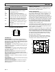
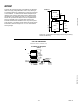
GENERAL INFORMATION
The ADP3367 contains a micropower bandgap reference volt-
age source, an error amplifier A1, two comparators (C1, C2)
and a series PNP output pass transistor.
CIRCUIT DESCRIPTION
The internal bandgap voltage reference is trimmed to 1.255V
and is used as a reference input to the error amplifier A1. The
feedback signal from the regulator output is supplied to the
other input by an on-chip voltage divider or by two external
resistors. When the SET input is at ground, the internal divider
provides the error amplifier’s feedback signal giving a +5V out-
put. When SET is at more than 50 mV above ground, compara-
tor C1 switches the error amplifier’s input directly to the SET
pin, and external resistors are used to set the output voltage.
The external resistors are selected so that the desired output
voltage gives 1.255 V at the SET input.
The output from the error amplifier supplies base current to the
PNP output pass transistor which provides output current. Up
to 300 mA output current is available provided that the device
power dissipation is not exceeded.
Comparator C2 compares the voltage on the Low Battery Input
(LBI) pin to the internal +1.255 V reference voltage. The out-
put from the comparator drives an open drain FET connected
to the Low Battery Output pin, LBO. The Low Battery Thresh-
old may be set using a suitable voltage divider connected to
LBI. When the voltage on LBI falls below 1.255 V, the open
drain output, LBO, is pulled low.
A shutdown (SHDN) input that can be used to disable the
error amplifier and hence the voltage output is also available.
The supply current in shutdown is less than 0.75 µA.
ADP3367
IN
SHDN
LBO
LBI
GND
50mV
SET
DD
OUT
1.255V
REF
A1
C1
C2
Figure 1. ADP3367 Functional Block Diagram