
Datasheet


ADP3367
–6–
REV. 0
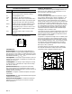
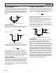
+
C1
10µF
IN
OUT
LBO
ADP3367
+5V
OUTPUT
R2
10kΩ
LBI
GNDSET SHDN
DROPOUT
STATUS
OUTPUT
DD
V
IN
R1
100kΩ
+
Figure 11. Dropout Status Output
Output Capacitor
An output capacitor is required on the ADP3367 to maintain sta-
bility and also to improve the load transient response. Capacitor
values from 10 µF upwards are recommended. Capacitors larger
than 10 µF will further improve the transient response. Tantalum
or aluminum electrolytics are suitable for most applications. For
temperatures below about –25°C, solid tantalums should be used
as many aluminum electrolytes freeze at this temperature.
Quiescent Current Considerations
The ADP3367 uses a PNP output stage to achieve low dropout
voltages combined with high output current capability. Under
normal regulating conditions the quiescent current is extremely
low. However if the input voltage drops so that it is below the
desired output voltage, the quiescent current increases consider-
ably. This happens because regulation can no longer be main-
tained and large base current flows in the PNP output transistor
in an attempt to hold it fully on. For minimum quiescent cur-
rent, it is therefore important that the input voltage is main-
tained higher than the desired output level. If the device is being
powered using a battery that can discharge down below the rec-
ommended level, there are a couple of techniques that can be
applied to reduce the quiescent current, but at the expense of
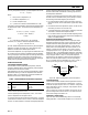
dropout voltage. The first of these is illustrated in Figure 12. By
connecting DD to SHDN the regulator is partially disabled with
input voltages below the desired output voltage and therefore
the quiescent current is reduced considerably.
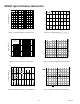
+
C1
10µF
IN OUT
ADP3367
+5V
OUTPUT
GNDSET SHDN
DD
V
IN
R1
47kΩ
+
C2
0.1µF
Figure 12. IQ Reduction 1
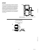
Another technique for reducing the quiescent current near drop-
out is illustrated in Figure 13. The DD output is used to modify
the output voltage so that as V
IN
drops, the desired output volt-
age setpoint also drops. This technique only works when exter-
nal resistors are used to set the output voltage. With V
IN
greater
than V
OUT
, DD has no effect. As V
IN
reduces and dropout is
reached, the DD output starts sourcing current into the SET
input through R3. This increases the SET voltage so that the
regulator feedback loop does not drive the internal PNP transis-
tor as hard as it otherwise would. As the input voltage continues
to decrease, more current is sourced, thereby reducing the PNP
drive even further. The advantage of this scheme is that it main-
tains a low quiescent current down to very low values of V
IN
at
which point the batteries are well outside their useful operating
range. The output voltage tracks the input voltage minus the
dropout. The SHDN function is also unaffected and may be
used normally if desired.
+
C1
10µF
IN OUT
ADP3367
+5V
OUTPUT
GND
SET
SHDN
DD
R1
610kΩ
R2
2MΩ
R3
1MΩ
+
V
IN
QUIESCENT CURRENT BELOW DROPOUT
0
1623 5
400
200
900
1mA
800
700
600
500µA
300
100
4
1.2mA
900µA
V
IN
– V
GROUND PIN CURRENT
Figure 13. IQ Reduction 2
POWER DISSIPATION
The ADP3367 can supply currents up to 300mA and can oper-
ate with input voltages as high as 16.5 V, but not simultaneously.
It is important that the power dissipation and hence the internal
die temperature be maintained below the maximum limits. Power
Dissipation is the product of the voltage differential across the
regulator times the current being supplied to the load. The
maximum package power dissipation is given in the Absolute
Maximum Ratings. In order to avoid excessive die temperatures,
these ratings must be strictly observed.
P
D
= (V
IN
– V
OUT
) (I
L
)
The die temperature is dependent on both the ambient tempera-
ture and on the power being dissipated by the device. The inter-
nal die temperature must not exceed 125°C. Therefore, care
must be taken to ensure that, under normal operating condi-
tions, the die temperature is kept below the thermal limit.
T
J
= T
A
+ P
D
(
θ
JA
)