
Datasheet
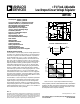


ADP3367
REV. 0
–7–
This may be expressed in terms of power dissipation as follows:
P
D
= (T
J
– T
A
)/(
θ
JA
)
where:
T
J
= Die Junction Temperature (°C)
T
A
= Ambient Temperature (°C)
P
D
= Power Dissipation (W)
θ
JA
= Junction to Ambient Thermal Resistance (°C/W)
If the device is being operated at the maximum permitted ambi-
ent temperature of 85°C, the maximum power dissipation per-
mitted is:
P
D
(max) = (T
J
(max) – T
A
)/(
θ
JA
)
P
D
(max) = (125 – 85)/(θ
JA
)
= 40/
θ
JA
where:
θ
JA
= 98°C/W for the 8-pin SOIC (R-8) package
Therefore, for a maximum ambient temperature of 85°C
P
D
(max) = 408 mW for R-8
At lower ambient temperatures the maximum permitted power
dissipation increases accordingly up to the maximum limits
specified in the absolute maximum specifications.
The thermal impedance (θ
JA
) figures given are measured in still
air conditions and are reduced considerably where fan assisted
cooling is employed. Other techniques for reducing the thermal
impedance include large contact pads on the printed circuit
board and wide traces. The copper will act as a heat exchanger
thereby reducing the effective thermal impedance.
POWER DISSIPATION
Low Thermal Resistance Package
The ADP3367 utilizes a patented and proprietary Thermal
Coastline Leadframe which offers significantly lower resistance
to heat flow from die to the PC board.
Heat generated on the die is removed and transferred to the PC
board faster resulting in lower die temperature than standard
packages. Table II is a performance comparison between and
standard and Thermal Coastline package.
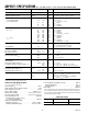
Table I. Thermal Resistance Performance Comparison*
Standard Package (SO-8) Thermal Coastline Package
θ
JC
44°C/W 40°C/W
θ
JA
170°C/W 98°C/W
PD 235 mW 408 mW
*Data presented in Table II is obtained using SEMI Standard Method G38-47
and SEMI Standard Specification G42-88.
A device operating at room temperature, +25°C, and +125°C
junction temperature can dissipate 1.15 W.
To maintain this high level of heat removal efficiency, once heat
is removed from the die to the PC board, it should be dissipated
to the air or other mediums to maintain the largest possible tem-
perature differential between the die and PC board; remember,
the rate at which heat is transferred is directly proportional to
the temperature differential.
Various PC board layout techniques could be used to remove
the heat from the immediate vicinity of the package. Consider
the following issues when designing a board layout:
1. PC board traces with larger copper cross section areas will
remove more heat; use PCs with thicker copper and/or wider
traces.
2. Increase the surface area exposed to open air so heat can be
removed by convection or forced air flow.
3. Use larger masses such as heat sinks or thermally conductive
enclosures to distribute and dissipate the heat.
4. Do not solder mask or silk screen the heat dissipating traces;
black anodizing will significantly improve heat dissipation by
means of increased radiation.
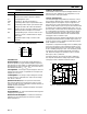
High Power Dissipation Recommendations
Where excessive power dissipation due to high input-output
differential voltages and/or high current conditions exists, the
simplest method of reducing the power requirements on the
regulator is to use a series dropper resistor. In this way the
excess power can be dissipated in the external resistor. As an
example, consider an input voltage of +12V and an output
voltage requirement of +5 V @ 100 mA with an ambient tem-
perature of +85°C. The package power dissipation under these
conditions is 700 mW which exceeds the maximum ratings. By
using a dropper resistor to drop 4 V, the power dissipation
requirement for the regulator is reduced to 300 mW which is
within the maximum specifications for the SO-8 package at
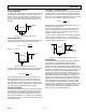
85°C. The resistor value is calculated as R = 4/0.1 = 40Ω.A
resistor power rating of 1/2 W or greater may be used.
IN
OUT
GNDSET SHDN
ADP3367
+5V
OUTPUT
C2
10µF
+
40Ω
0.5W
C1
1µF
V
IN
12V
+
Figure 14. Reducing Regulator Power Dissipation
Transient Response
The ADP3367 exhibits excellent transient performance as illus-
trated in the “Typical Performance Characteristics.” Figure 6
shows that an input step from 10 V to 6 V results in a very small
output disturbance (50 mV). Adding an input capacitor would
improve this even more.
Figure 7 shows how quickly the regulator recovers from an out-
put load change from 10 mA to 100 mA. The offset due to the
load current change is less than 1 mV.
Monitored µP Power Supply
Figure 15 shows the ADP3367 being used in a monitored µP
supply application. The ADP3367 supplies +5V for the micro-