
Datasheet

Dual 3 MHz, 800 mA Buck
Regulators with Two 300 mA LDOs
Data Sheet
ADP5033
Rev. F Document Feedback
Information furnished by Analog Devices is believed to be accurate and reliable. However, no
responsibility is assumed by Analog Devices for its use, nor for any infringements of patents or other
rights of third parties that may result from its use. Specifications subject to change without notice. No
license is granted by implication or otherwise under any patent or patent rights of Analog Devices.
Trademarks and registered trademarks are the property of their respective owners.
One Technology Way, P.O. Box 9106, Norwood, MA 02062-9106, U.S.A.
Tel: 781.329.4700 ©2011–2013 Analog Devices, Inc. All rights reserved.
Technical Support www.analog.com
FEATURES
Main input voltage range: 2.3 V to 5.5 V
Two 800 mA buck regulators and two 300 mA LDOs
Tiny, 16-ball, 2 mm × 2 mm WLCSP package
Regulator accuracy: ±1.8%
Factory programmable VOUTx
3 MHz buck operation with forced PWM and auto PWM/PSM
modes
BUCK1/BUCK2: output voltage range from 0.8 V to 3.8 V
LDO1/LDO2: output voltage range from 0.8 V to 5.2 V
LDO1/LDO2: low input supply voltage from 1.7 V to 5.5 V
LDO1/LDO2: high PSRR and low output noise
APPLICATIONS
Power for processors, ASICS, FPGAs, and RF chipsets
Portable instrumentation and medical devices
Space constrained devices
GENERAL DESCRIPTION
The ADP5033 combines two high performance buck regulators
and two low dropout regulators (LDO) in a tiny, 16-ball, 2 mm ×
2 mm WLCSP to meet demanding performance and board
space requirements.
The high switching frequency of the buck regulators enables tiny
multilayer external components and minimizes the board space.
When the MODE pin is set high, the buck regulators operate in
forced PWM mode. When the MODE pin is set low, the buck
regulators operate in PWM mode when the load current is above
a predefined threshold. When the load current falls below a
predefined threshold, the regulator operates in power save
mode (PSM), improving the light load efficiency.
The two bucks operate out of phase to reduce the input capacitor
requirement and noise.
The low quiescent current, low dropout voltage, and wide input
voltage range of the ADP5033 LDO extend the battery life of
portable devices. The ADP5033 LDOs maintain power supply
rejection greater than 60 dB for frequencies as high as 10 kHz
while operating with a low headroom voltage.
The regulators in the ADP5033 are activated by the ENA and ENB
pins. The specific channels controlled by ENA and ENB are set
by factory programming. A high voltage level applied to the enable
pins activates the regulators. The default output voltages are
factory programmable and can be set to a wide range of options.
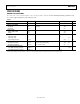
Table 1. Family Models
Model Channels
Maximum
Current Package
ADP5023 2 Buck, 1 LDO 800 mA, 300 mA LFCSP (CP-24-10)
ADP5024 2 Buck, 1 LDO 1.2 A, 300 mA LFCSP (CP-24-10)
ADP5034 2 Buck, 2 LDOs 1.2 A, 300 mA LFCSP (CP-24-10),
TSSOP (RE-28-1)
ADP5037 2 Buck, 2 LDOs 800 mA,
300 mA
LFCSP (CP-24-10)
ADP5033 2 Buck, 2 LDOs
with 2 EN pins
800 mA,
300 mA
WLCSP (CB-16-8)
ADP5040 1 Buck, 2 LDOs 1.2 A, 300 mA LFCSP (CP-20-10)
ADP5041 1 Buck, 2 LDOs w/
Supervisory,
Watchdog, Manual
Reset
1.2 A, 300 mA LFCSP (CP-20-10)
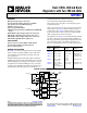
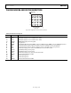
TYPICAL APPLICATION CIRCUIT
VIN1
2.3V TO 5.5V
SW1
VOUT1
PGND1
MODE
C5
10µF
L1 1µH
BUCK1
C2
4.7µF
C1
4.7µF
VIN2
AGND
BUCK2
SW2
VOUT2
PGND2
C6
10µF
L2 1µH
VOUT3
C7
1µF
VOUT4
C8
1µF
VIN3
C3
1µF
1.7V TO 5.5V
LDO1
(ANALOG)
VIN4
C4
1µF
ADP5033
ENA
ACTIV. AND
UVLO
ENB
ON
OFF
PSM/PWM
PWM
EN1
EN2
EN3
EN4
LDO2
(DIGITAL)
EN2
EN3
EN4
MODE
MODE
VOUT1 @
800mA
VOUT2 @
800mA
VOUT3 @
300mA
VOUT4 @
300mA
09788-001
Figure 1.