
Datasheet

ADP5033 Data Sheet
Rev. F | Page 2 of 28
TABLE OF CONTENTS
Features .............................................................................................. 1
Applications ....................................................................................... 1
General Description ......................................................................... 1
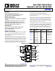
Typical Application Circuit ............................................................. 1
Revision History ............................................................................... 2
Specifications ..................................................................................... 3
General Specifications ................................................................. 3
BUCK1 and BUCK2 Specifications ........................................... 4
LDO1 and LDO2 Specifications ................................................. 4
Input and Output Capacitor, Recommended Specifications .. 5
Absolute Maximum Ratings ............................................................ 6
Thermal Resistance ...................................................................... 6
ESD Caution .................................................................................. 6
Pin Configuration and Function Descriptions ............................. 7
Typical Performance Characteristics ............................................. 8
Theory of Operation ...................................................................... 15
Power Management Unit ........................................................... 15
BUCK1 and BUCK2 .................................................................. 16
LDO1 and LDO2 ........................................................................ 17
Applications Information .............................................................. 18
Buck External Component Selection ....................................... 18
LDO Capacitor Selection .......................................................... 20
Power Dissipation and Thermal Considerations ....................... 21
Buck Regulator Power Dissipation .......................................... 21
Junction Temperature ................................................................ 22
PCB Layout Guidelines .................................................................. 23
Typical Application Schematic ..................................................... 24
Outline Dimensions ....................................................................... 25
Ordering Guide .......................................................................... 26
REVISION HISTORY
10/13—Rev. E to Rev. F
Changes to VIN1 Undervoltage Lockout Parameter, Table 2 ...... 3
Changes to Undervoltage Lockout Section .................................. 16
Moved Ordering Guide ................................................................... 26
Changes to Ordering Guide ........................................................... 26
9/13—Rev. D to Rev. E
Changes to Table 1 ............................................................................. 1
Changes to Ordering Guide ........................................................... 25
5/13—Rev. C to Re v. D
Added Table 1; Renumbered Sequentially .................................... 1
Changes to Ordering Guide .......................................................... 25
1/13—Rev. B to Re v. C
Changes to Figure 9 .......................................................................... 9
Changes to Ordering Guide .......................................................... 25
10/12—Rev. A to Re v. B
Changes to Features Section............................................................ 1
Changes to Buck Output Voltage Accuracy Parameter, Table 2 .. 4
Changes to LDO Output Voltage Accuracy Parameter, Table 3 .. 4
Changes to Figure 6 to Figure 8 ...................................................... 8
Changes to Figure 30 to Figure 32 ................................................ 12
Changes to Figure 36 Caption ....................................................... 13
Changes to Undervoltage Lockout Section ................................. 16
Moved Power Dissipation and Thermal Considerations
Section .............................................................................................. 21
Changes to Buck Regulator Power Dissipation Section ............ 21
Updated Outline Dimensions ....................................................... 25
Changes to Ordering Guide .......................................................... 25
1/12—Rev. 0 to Re v. A
Changes to Features Section and General Description Section .... 1
Changes to Output Characteristics Parameter, Table 2 ................ 4
Changes to Output Characteristics Parameter, Table 3 and
Dropout Voltage Parameter, Table 3 ............................................... 4
Changes to Nominal Input and Output Capacitor Ratings
Parameter, Table 4 ............................................................................. 5
Changes to Table 5 ............................................................................. 6
Changed V
IN1
= V
IN2
= V
IN3
= V
IN4
= 5.0 V to V
IN1
= V
IN2
= V
IN3
=
V
IN4
= 3.6 V ......................................................................................... 8
Changes to Figure 4 to Figure 8 ....................................................... 8
Change to Figure 15 Caption and Figure 17 Caption ................ 10
Changes Figure 19 and Figure 20 ................................................. 10
Changes to Figure 31 and Figure 32............................................. 12
Changes to Figure 33, Figure 37, and Figure 38 ......................... 13
Changes to Buck Regulator Power Dissipation Section ............ 15
Changes to LDO Regulator Power Dissipation Section and
Junction Temperature Section ...................................................... 16
Changes to Undervoltage Lockout Section ................................. 18
Changes to LDO1 and LDO2 Section ......................................... 19
Changes to Output Capacitor Section ......................................... 20
Changes to Table 9 .......................................................................... 21
Change to Input and Output Capacitor Properties Section ..... 22
Changes to Ordering Guide .......................................................... 25
5/11—Revision 0: Initial Version