
Datasheet
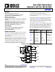

ADP5033 Data Sheet
Rev. F | Page 4 of 28
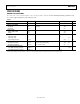
BUCK1 AND BUCK2 SPECIFICATIONS
V
IN1
= V
IN2
= 2.3 V to 5.5 V; T
J
= −40°C to +125°C for minimum/maximum specifications, and T
A
= 25°C for typical specifications, unless
otherwise noted.
1
Table 3.
Parameter Symbol Test Conditions/Comments Min Typ Max Unit
INPUT CHARACTERISTICS
Input Voltage Range V
IN1
, V
IN2
PWM mode, I
LOAD1
= I
LOAD2
= 0 mA to 800 mA 2.3 5.5 V
OUTPUT CHARACTERISTICS
Output Voltage Accuracy ∆V
OUT1
/V
OUT1
, ∆V
OUT2
/V
OUT2
PWM mode; I
LOAD1
= I
LOAD2
= 0 mA −1.8 +1.8 %
Line Regulation
(∆V
OUT1
/V
OUT1
)/∆V
IN1
,
(∆V
OUT2
/V
OUT2
)/∆V
IN2
PWM mode −0.05 %/V
Load Regulation
(∆V
OUT1
/V
OUT1
)/∆I
OUT1
,
(∆V
OUT2
/V
OUT2
)/∆I
OUT2
I
LOAD
= 0 mA to 800 mA, PWM mode −0.1 %/A
PSM CURRENT THRESHOLD
PSM to PWM Operation I
PSM
100 mA
OPERATING SUPPLY CURRENT MODE = ground
BUCK1 Only I
IN
I
LOAD1
= 0 mA, device not switching, all
other channels disabled
44 μA
BUCK2 Only
I
IN
I
LOAD2
= 0 mA, device not switching, all
other channels disabled
55
μA
BUCK1 and BUCK2 I
IN
I
LOAD1
= I
LOAD2
= 0 mA, device not switching,
LDO channels disabled
67 μA
SW CHARACTERISTICS
SW On Resistance R
PFET
PFET at VIN1 = 5 V 145 235 mΩ
R
PFET
PFET at VIN1 = 3.6 V 180 295 mΩ
R
NFET
NFET at VIN1 = 5 V 110 190 mΩ
R
NFET
NFET at VIN1 = 3.6 V
125
220
mΩ
Current Limit I
LIMIT1
, I
LIMIT2
PFET switch peak current limit 1100 1350 mA
ACTIVE PULL-DOWN R
PDWN-B
Channel disabled 75 Ω
OSCILLATOR FREQUENCY f
SW
2.5 3.0 3.5 MHz
1
All limits at temperature extremes are guaranteed via correlation using standard statistical quality control (SQC).
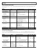
LDO1 AND LDO2 SPECIFICATIONS
V
IN3
= (V
OUT3
+ 0.5 V) or 1.7 V (whichever is greater) to 5.5 V, V
IN4
= (V
OUT4
+ 0.5 V) or 1.7 V (whichever is greater) to 5.5 V; C
IN
= C
OUT
=
1 µF; T
J
= −40°C to +125°C for minimum/maximum specifications, and T
A
= 25°C for typical specifications, unless otherwise noted.
1
Table 4.
Parameter Symbol Test Conditions/Comments Min Typ Max Unit
INPUT VOLTAGE RANGE V
IN3
, V
IN4
1.7 5.5 V
OPERATING SUPPLY CURRENT
Bias Current per LDO
2
I
VIN3BIAS
/I
VIN4BIAS
I
OUT3
= I
OUT4
= 0 µA 10 30 µA
I
OUT3
= I
OUT4
= 10 mA 60 100 µA
I
OUT3
= I
OUT4
= 300 mA 165 245 µA
Total System Input Current I
IN
Includes all current into VIN1, VIN2, VIN3, and VIN4
LDO1 or LDO2 Only I
OUT3
= I
OUT4
= 0 µA, all other channels disabled 53 µA
LDO1 and LDO2 Only I
OUT3
= I
OUT4
= 0 µA, buck channels disabled 74 µA
OUTPUT CHARACTERISTICS
Output Voltage Accuracy
∆V
OUT3
/V
OUT3
,
∆V
OUT4
/V
OUT4
100 µA < I
OUT3
< 300 mA, 100 µA < I
OUT4
< 300 mA −1.8 +1.8 %
Line Regulation
(∆V
OUT3
/V
OUT3
)/∆V
IN3
,
(∆V
OUT4
/V
OUT4
)/∆V
IN4
I
OUT3
= I
OUT4
= 1 mA −0.03 +0.03 %/V
Load Regulation
3
(∆V
OUT3
/V
OUT3
)/∆I
OUT3
,
(∆V
OUT4
/V
OUT4
)/∆I
OUT4
I
OUT3
= I
OUT4
= 1 mA to 300 mA 0.001 0.003 %/mA