
Datasheet
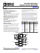

Data Sheet ADP5033
Rev. F | Page 5 of 28
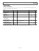
Parameter Symbol Test Conditions/Comments Min Typ Max Unit
DROPOUT VOLTAGE
4
V
DROPOUT
V
OUT3
= V
OUT4
= 5.2 V, I
OUT3
= I
OUT4
= 300 mA 50 mV
V
OUT3
= V
OUT4
= 3.3 V, I
OUT3
= I
OUT4
= 300 mA 65 110 mV
V
OUT3
= V
OUT4
= 2.5 V, I
OUT3
= I
OUT4
= 300 mA 85 mV
V
OUT3
= V
OUT4
= 1.8 V, I
OUT3
= I
OUT4
= 300 mA 165 mV
CURRENT-LIMIT THRESHOLD
5
I
LIMIT3
, I
LIMIT4
335 600 mA
ACTIVE PULL-DOWN R
PDWN-L
Channel disabled 600 Ω
POWER SUPPLY REJECTION RATIO PSRR
Regulator LDO1
10 kHz, V
IN3
= 3.3 V, V
OUT3
= 2.8 V, I
OUT3
= 1 mA
60
dB
100 kHz, V
IN3
= 3.3 V, V
OUT3
= 2.8 V, I
OUT3
= 1 mA 62 dB
1 MHz, V
IN3
= 3.3 V, V
OUT3
= 2.8 V, I
OUT3
= 1 mA 63 dB
Regulator LDO2 10 kHz, V
IN4
= 1.8 V, V
OUT4
= 1.2 V, I
OUT4
= 1 mA 54 dB
100 kHz, V
IN4
= 1.8 V, V
OUT4
= 1.2 V, I
OUT4
= 1 mA 57 dB
1 MHz, V
IN4
= 1.8 V, V
OUT4
= 1.2 V, I
OUT4
= 1 mA 64 dB
1
All limits at temperature extremes are guaranteed via correlation using standard statistical quality control (SQC).
2
This is the input current into VIN3/VIN4, which is not delivered to the output load.
3
Based on an endpoint calculation using 1 mA and 300 mA loads.
4
Dropout voltage is defined as the input-to-output voltage differential when the input voltage is set to the nominal output voltage. This applies only to output voltages
above 1.7 V.
5
Current-limit threshold is defined as the current at which the output voltage drops to 90% of the specified typical value. For example, the current limit for a 3.0 V
output voltage is defined as the current that causes the output voltage to drop to 90% of 3.0 V, or 2.7 V.
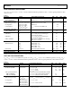
INPUT AND OUTPUT CAPACITOR, RECOMMENDED SPECIFICATIONS
T
A
= −40°C to +125°C, unless otherwise specified.
Table 5.
Parameter Symbol Min Typ Max Unit
NOMINAL INPUT AND OUTPUT CAPACITOR RATINGS
BUCK1, BUCK2 Input Capacitor Rating C
MIN1
, C
MIN2
4.7 40 µF
BUCK1, BUCK2 Output Capacitor Rating C
MIN1
, C
MIN2
10 40 µF
LDO1, LDO2
1
Input and Output Capacitor Rating C
MIN3
, C
MIN4
1.0 µF
CAPACITOR ESR R
ESR
0.001 1 Ω
1
The minimum input and output capacitance should be greater than 0.70 µF over the full range of operating conditions. The full range of operating conditions in the
application must be considered during device selection to ensure that the minimum capacitance specification is met. X7R- and X5R-type capacitors are
recommended; Y5V and Z5U capacitors are not recommended for use because of their poor temperature and dc bias characteristics.