
Datasheet

ADP5033 Data Sheet
Rev. F | Page 6 of 28
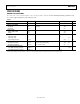
ABSOLUTE MAXIMUM RATINGS
Table 6.
Parameter Rating
VIN1 to AGND −0.3 V to +6 V
VIN2 to VIN1
−0.3 V to +0.3 V
PGND1, PGND2 to AGND −0.3 V to +0.3 V
VIN3, VIN4, VOUT1, VOUT2, ENA, ENB,
MODE to AGND
−0.3 V to
(VIN1 + 0.3 V)
VOUT3 to AGND
−0.3 V to
(VIN3 + 0.3 V)
VOUT4 to AGND
−0.3 V to
(VIN4 + 0.3 V)
SW1 to PGND1
−0.3 V to
(VIN1 + 0.3 V)
SW2 to PGND2
−0.3 V to
(VIN2 + 0.3 V)
Storage Temperature Range −65°C to +150°C
Operating Junction Temperature Range −40°C to +125°C
Soldering Conditions JEDEC J-STD-020
Stresses above those listed under Absolute Maximum Ratings
may cause permanent damage to the device. This is a stress
rating only; functional operation of the device at these or any
other conditions above those indicated in the operational
section of this specification is not implied. Exposure to absolute
maximum rating conditions for extended periods may affect
device reliability.
For detailed information on power dissipation, see the Power
Dissipation and Thermal Considerations section.
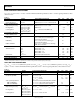
THERMAL RESISTANCE
θ
JA
and Ψ
JB
are specified for the worst-case conditions, that is, a
device soldered in a circuit board for surface-mount packages.
Table 7. Thermal Resistance
Package Type θ
JA
Ψ
JB
Unit
16-Ball, 0.5 mm Pitch WLCSP 57 14 °C/W
ESD CAUTION