
Datasheet

Data Sheet ADP5033
Rev. F | Page 7 of 28
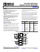
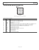
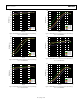
PIN CONFIGURATION AND FUNCTION DESCRIPTIONS
TOP VIEW
(BALL SIDE DOWN)
Not to Scale
1
A
B
C
D
2 3 4
BALL A1
INDICATOR
VOUT3
AGND
VIN1
PGND1
VIN4
ENA
VOUT2
SW2
VOUT4
ENB
VIN2
PGND2
VIN3
MODE
VOUT1
SW1
09788-002
Figure 2. Pin Configuration—View from the Top of the Die
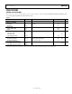
Table 8. Pin Function Descriptions
Pin No. Mnemonic Description
A1 VOUT3 LDO1 Output Voltage and Sensing Input.
A2 VIN3 LDO1 Input Supply (1.7 V to 5.5 V, VIN4 ≤ VIN1 = VIN2).
A3 VIN4 LDO2 Input Supply (1.7 V to 5.5 V, VIN3 ≤ VIN1 = VIN2).
A3 VOUT4 LDO2 Output Voltage and Sensing Input.
B1 AGND Analog Ground.
B2 MODE BUCK1/BUCK2 Operating Mode. MODE = high: forced PWM operation. MODE = low: auto PWM/PSM operation.
B3 ENA Regulator Enable Pin A, Active High. The regulators turned on with ENA are factory programmed.
B4 ENB Regulator Enable Pin B, Active High. The regulators turned on with ENB are factory programmed.
C1 VIN1 BUCK1 Input Supply (2.3 V to 5.5 V) and UVLO Detection. Connect VIN1 to VIN2.
C2 VOUT1 BUCK1 Output Voltage Sensing Input.
C3
VOUT2
BUCK2 Output Voltage Sensing Input.
C4 VIN2 BUCK2 Input Supply (2.3 V to 5.5 V). Connect VIN2 to VIN1.
D1 PGND1 Dedicated Power Ground for BUCK1.
D2 SW1 BUCK1 Switching Node.
D3 SW2 BUCK2 Switching Node.
D4 PGND2 Dedicated Power Ground for BUCK2.