
Datasheet


ADP5034 Data Sheet
Rev. E | Page 2 of 28
TABLE OF CONTENTS
Features .............................................................................................. 1
Applications ....................................................................................... 1
General Description ......................................................................... 1
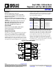
Typical Application Circuit ............................................................. 1
Revision History ............................................................................... 3
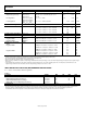
Specifications ..................................................................................... 4
General Specifications ................................................................. 4
BUCK1 and BUCK2 Specifications ........................................... 5
LDO1 and LDO2 Specifications ................................................. 5
Input and Output Capacitor, Recommended Specifications .. 6
Absolute Maximum Ratings ............................................................ 7
Thermal Resistance ...................................................................... 7
ESD Caution .................................................................................. 7
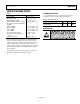
Pin Configuration and Function Descriptions ............................. 8
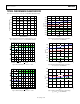
Typical Performance Characteristics ............................................. 9
Theory of Operation ...................................................................... 16
Power Management Unit ........................................................... 16
BUCK1 and BUCK2 .................................................................. 18
LDO1 and LDO2 ........................................................................ 19
Applications Information .............................................................. 20
Buck External Component Selection ....................................... 20
LDO External Component Selection....................................... 22
Power Dissipation and Thermal Considerations ....................... 23
Buck Regulator Power Dissipation .......................................... 23
Junction Temperature ................................................................ 24
PCB Layout Guidelines .................................................................. 25
Typical Application Schematics .................................................... 26
Bill of Materials ........................................................................... 26
Outline Dimensions ....................................................................... 27
Ordering Guide .......................................................................... 28