
Datasheet


ADP5034 Data Sheet
Rev. E | Page 8 of 28
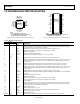
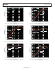
PIN CONFIGURATION AND FUNCTION DESCRIPTIONS
PIN 1
INDICATOR
NOTES
1. NC = NOT INTERNALLY CONNECTED.
2. IT IS RECOMMENDED THAT THE EXPOSED PAD
BE SOLDERED TO THE GROUND PLANE.
1
2
3
4
5
6
15
16
17
18
14
13
7
8
9
11
12
10
21
22
23
24
20
19
ADP5034
TOP VIEW
(Not to Scale)
VOUT4
FB3
VOUT3
VIN3
EN3
VIN4
AGND
AVIN
VIN1
SW1
PGND1
MODE
FB4
EN4
VIN2
SW2
PGND2
NC
EN1
FB1
VOUT1
VOUT2
FB2
EN2
09703-003
Figure 2. LFCSP Pin Configuration—View from the Top of the Die
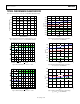
09703-100
1
2
3
4
5
6
7
8
9
10
11
12
13
14
28
27
26
25
24
23
22
21
20
19
18
17
16
15
VIN4
VOUT4
NC
VIN2
EN4
FB4
EN3
VOUT3
FB3
NC
VIN1
AVIN
AGND
SW2
PGND2
NC
FB2
VOUT2
EN2
NC
SW1
PGND1
MODE
FB1
VOUT1
EN1
NC
VIN3
TOP VIEW
(Not to Scale)
ADP5034
NOTES
1. NC = NOT INTERNALLY CONNECTED.
2. IT IS RECOMMENDED THAT THE EXPOSED PAD BE
SOLDERED TO THE GROUND PLANE.
Figure 3. TSSOP Pin Configuration—View from the Top of the Die
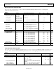
Table 8. Pin Function Descriptions
Pin No.
Mnemonic Description
LFCSP TSSOP
1 5 FB4 LDO2 Feedback Input. For device models with an adjustable output voltage, connect this pin to the
middle of the LDO2 resistor divider. For device models with a factory programmed output voltage,
connect FB4 to the top of the capacitor on VOUT4.
2 6 EN4 LDO2 Enable Pin. High level turns on this regulator, and low level turns it off.
3 7 VIN2 BUCK2 Input Supply (2.3 V to 5.5 V). Connect VIN2 to VIN1 and AVIN.
4 8 SW2 BUCK2 Switching Node.
5 9 PGND2 Dedicated Power Ground for BUCK2.
6 4, 10, 11,
18, 25
NC No Connect. Leave this pin unconnected or connect to ground.
7
12
EN2
BUCK2 Enable Pin. High level turns on this regulator, and low level turns it off.
8 13 FB2 BUCK2 Feedback Input. For device models with an adjustable output voltage, connect this pin to the
middle of the BUCK2 resistor divider. For device models with a fixed output voltage, leave this pin
unconnected.
9 14 VOUT2 BUCK2 Output Voltage Sensing Input. Connect VOUT2 to the top of the capacitor on VOUT2.
10 15 VOUT1 BUCK1 Output Voltage Sensing Input. Connect VOUT1 to the top of the capacitor on VOUT1.
11 16 FB1 BUCK1 Feedback Input. For device models with an adjustable output voltage, connect this pin to the
middle of the BUCK1 resistor divider. For device models with a fixed output voltage, leave this pin
unconnected.
12 17 EN1 BUCK1 Enable Pin. High level turns on this regulator, and low level turns it off.
13 19 MODE BUCK1/BUCK2 Operating Mode. MODE = high: forced PWM operation. MODE = low: auto PWM/PSM
operation.
14 20 PGND1 Dedicated Power Ground for BUCK1.
15
21
SW1
BUCK1 Switching Node.
16 22 VIN1 BUCK1 Input Supply (2.3 V to 5.5 V). Connect VIN1 to VIN2 and AVIN.
17 23 AVIN Analog Input Supply (2.3 V to 5.5 V). Connect AVIN to VIN1 and VIN2.
18 24 AGND Analog Ground.
19 26 FB3 LDO1 Feedback Input. For device models with an adjustable output voltage, connect this pin to the
middle of the LDO1 resistor divider. For device models with a factory programmed output voltage,
connect FB3 to the top of the capacitor on VOUT3.
20 27 VOUT3 LDO1 Output Voltage.
21 28 VIN3 LDO1 Input Supply (1.7 V to 5.5 V).
22 1 EN3 LDO1 Enable Pin. High level turns on this regulator, and low level turns it off.
23 2 VIN4 LDO2 Input Supply (1.7 V to 5.5 V).
24 3 VOUT4 LDO2 Output Voltage.
EPAD EPAD EP Exposed Pad. It is recommended that the exposed pad be soldered to the ground plane.