
Datasheet


Fast Charge Battery Manager with Power
Path and USB Compatibility
Data Sheet
ADP5065
Rev. D Document Feedback
Information furnished by Analog Devices is believed to be accurate and reliable. However, no
responsibility is assumed by Analog Devices for its use, nor for any infringements of patents or other
rights of third parties that may result from its use. Specifications subject to change without notice. No
license is granted by implication or otherwise under any patent or patent rights of Analog Devices.
Trademarks and registered trademarks are the property of their respective owners.
One Technology Way, P.O. Box 9106, Norwood, MA 02062-9106, U.S.A.
Tel: 781.329.4700 ©2011–2013 Analog Devices, Inc. All rights reserved.
Technical Support www.analog.com
FEATURES
3 MHz switch mode charger
1.25 A charge current from dedicated charger
Up to 680 mA charging current from 500 mA USB host
Operating input voltage from 4.0 V up to 5.5 V
Tolerant input voltage −0.5 V to +20 V (USB VBUS)
Dead battery isolation FET between battery and
charger output
Battery thermistor input with automatic charger shutdown
for when battery temperature exceeds limits
Compliant with the JEITA Li-Ion battery charging
temperature specification
SYS_EN_OK flag to hold off system turn-on until battery is at
minimum required level for guaranteed system startup
due to minimum battery voltage and/or minimum battery
charge level requirements
EOC programming with C/20, C/10 and specific current level
selection
APPLICATIONS
Digital still cameras
Digital video cameras
Single cell Li-Ion portable equipment
PDA, audio, GPS devices
Mobile phones
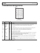
FUNCTIONAL BLOCK DIAGRAM
V_WEAK_SET AGND
PGNDx
IIN_EXT
TRK_EXT
SCL
SDA
SYS_ON_OK
CHARGER
CONTROL
BLOCK
3MHz
BUCK
CFILT
VBUS
AC
OR
USB
VINx
PGNDx
ISO_Sx
ISO_Bx
BAT_SNS
THR
SWx
INDUCTOR
SYSTEM
+
Li-Ion
ADP5065
09370-001
Figure 1.
GENERAL DESCRIPTION
The ADP5065 charger is fully compliant with the USB 2.0,
USB 3.0, and USB Battery Charging Specification 1.1 and
enables charging via the mini USB VBUS pin from a wall
charger, car charger, or USB host port.
The ADP5065 operates from a 4 V to 5.5 V input voltage range
but is tolerant of voltages of up to 20 V. T h is alleviates the
concerns about the USB bus spiking during disconnect or
connect scenarios.
The ADP5065 also features an internal FET between the dc-to-
dc charger output and the battery. This permits battery isolation
and, hence, system powering under a dead battery or no battery
scenario, which allows for immediate system function on
connection to a USB power supply.
Based on the type of USB source, which is detected by an external
USB detection chip, the ADP5065 can be set to apply the correct
current limit for optimal charging and USB compliance.
The ADP5065 comes in a very small and low profile 20-lead
WLCSP (0.5 mm pitch spacing) package.
The overall solution requires only five small, low profile external
components consisting of four ceramic capacitors (one of which
is the battery filter capacitor), one multilayer inductor. In addition
to these components, there is one optional dead battery situation
default setting resistor. This configuration enables a very small
PCB area to provide an integrated and performance enhancing
solution to USB battery charging and power rail provision.