
Datasheet


Data Sheet ADP5065
Rev. D | Page 7 of 40
ABSOLUTE MAXIMUM RATINGS
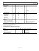
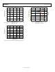
Table 4.
Parameter Rating
VIN1, VIN2 to PGND1, PGND2
−0.5 V to +20 V
All Other Pins to AGND −0.3 V to +6 V
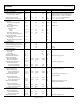
Continuous Drain Current, Battery Supple-
mentary Mode, from ISO_Bx to ISO_Sx
T
J
≤ 85°C 2.2 A
T
J
= 125°C 1.1 A
Storage Temperature Range −65°C to +150°C
Operating Junction Temperature Range −40°C to +125°C
Soldering Conditions JEDEC J-STD-020
Stresses a bove those listed under Absolute Maximum Ratings
may cause permanent damage to the device. This is a stress
rating only; functional operation of the device at these or any
other conditions above those indicated in the operational
section of this specification is not implied. Exposure to absolute
maximum rating conditions for extended periods may affect
device reliability.
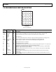
THERMAL RESISTANCE
θ
JA
is specified for the worst-case conditions, that is, a device
soldered in a circuit board for surface-mount packages.
Table 5. Thermal Resistance
Package Type θ
JA
θ
JC
θ
JB
Unit
20-Lead WLCSP
1
46.8 0.7 9.2 °C/W
1
5 × 4 array, 0.5 mm pitch (2.75 mm × 2.08 mm); based on a JEDEC, 2S2P,
4-layer board with 0 m/sec airflow.
Maximum Power Dissipation
The maximum safe power dissipation in the ADP5065 package
is limited by the associated rise in junction temperature (T
J
) on
the die. At approximately 150°C, which is the glass transition
temperature, the plastic changes its properties. Even temporarily
exceeding this temperature limit may change the stresses that
the package exerts on the die, permanently shifting the para-
metric performance of the ADP5065. Exceeding a junction
temperature of 175°C for an extended period of time can result
in changes in the silicon devices that potentially cause failure.
ESD CAUTION